This thread has been locked.

If you have a related question, please click the "Ask a related question" button in the top right corner. The newly created question will be automatically linked to this question.

CCS: ADXL362 with MSP430F5529LP

Other Parts Discussed in Thread: MSP430F5529, MSP430F6779

Tool/software: Code Composer Studio

HI,

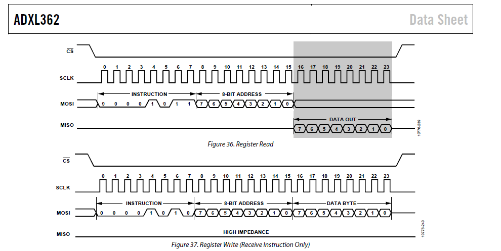
        i have interfaced adxl362 to the msp430f5529 lp using the spi interface (USCI A0) and am trying to read the device id of the adxl ic but there is no output, please help me with the code and also want to write to the adxl362 register, so how should i proceed with as well?

below is the code

#include "msp430.h"
#include <msp430f5529.h>


int i,k;

char devid,dataform;

unsigned char read_byte(unsigned char byte)
{
	UCA0IFG &= ~UCRXIFG;
	UCA0TXBUF = byte;
	while(!(UCA0STAT & UCBUSY));
    UCA0TXBUF = 0xff;
    while(!(UCA0STAT & UCBUSY));
	return UCA0RXBUF;
}


void main(void)

{
	WDTCTL = WDTPW+WDTHOLD;                   // Stop watchdog timer

P3SEL |= BIT3+BIT4;                       // P3.3,4 option select
  P2SEL |= BIT7;                            // P2.7 option select

  UCA0CTL1 |= UCSWRST;                      // **Put state machine in reset**
  UCA0CTL0 |= UCMST+UCSYNC+UCCKPL+UCMSB;    // 3-pin, 8-bit SPI master
                                            // Clock polarity high, MSB
  UCA0CTL1 |= UCSSEL_2;                     // SMCLK
  UCA0BR0 = 0x02;                           // /2
  UCA0BR1 = 0;                              //
  UCA0MCTL = 0;                             // No modulation
  UCA0CTL1 &= ~UCSWRST;                     // **Initialize USCI state machine**
  UCA0IE |= UCRXIE;                         // Enable USCI_A0 RX interrupt

  P3OUT &= ~BIT2;
  read_byte(0x0B);                  /// command to read
 devid = read_byte(0x00);                  //address to read


  P3OUT |= BIT2;
}

  • Hello,
    I will move this thread to the MSP forums. The experts there can help you best.

    Thanks
    ki
  • Hi Pratiksha,

    You never set the chip select (CS) pin to the output direction (P3DIR |= BIT2;) therefore that pin is in input mode and most likely not driving the CS pin low. According to Figure 41 of the ADXL362 datasheet SCLK is inactive low and data is captured on the first edge (rising). UCCKPH should be set instead of UCCKPL to match the expected clock settings.

    Regards,
    Ryan
  • thank you for the help

    Pratiksha bhuta
  • Hello,

    I have set the CS pin and the SCLK as per your suggestion but still i am not able to read the device id , please help me
  • Re-read the ADXL362 datasheet concerning SPI communication, Figures 36 through 42 are particularly important. For example, reading the device ID register requires sending an instruction (0x0B), and 8-bit address (0x00), and a dummy byte (0xFF) in which case RXBUF is then populated. Past this you need to re-check your hardware connections and debug the communication lines with an oscilloscope or logic analyzer.

    Regards,
    Ryan
  • hello pratiksha,

                   what do you mean by there is no output what did you get on SOMI line. Have you checked on oscilloscope???. try debug your code using following steps and use oscilloscope.

    1) do spi initialization.[(UCA0CTL0 |= UCMST+UCSYNC+UCMSB) why are you using UCCKPL].

         after initialization,  transmit some garbage value continuously on SIMO line and check the DATA(SIMO) & CLOCK on oscilloscope if  you see what you are actually sending then initialization is correct.


    eg:


     WDTCTL = WDTPW | WDTHOLD;
    
           pin_init();
    
           clock_select(meg_16);
    
           spi_init();
    
           __bis_SR_register(GIE);
    
    while(1)
    
    {
    
        while (!(IFG2 & UCB0TXIFG));
    
        UCB0TXBUF = 0x81;
    
        __delay_cycles(100);
    
    }

    when initialization ok move on to next step.

    2) now check the datasheet of adxl362 and try to send frame for reading device id(as you had already done in your above code)

       Send the command continuously with a minor delay so that you get continuous response on SOMI line then check the response on oscilloscope.

       if getting wrong response then try different combination of (UCCKPH & UCCKPL) in SPI initialization step.

       first step is to get a response from slave whether right or wrong :)

    Note : I am not an expert i am just a student. but i have interfaced( different adc's , can controller , serial flash)  using spi module of msp430f6779 . i always follow these steps and usually gets the result..

       now time to interface accelerometer  as well :)

  • hey,

             i modified the code as per your guideline but when i see the signals on oscilloscope i see clock for just a fraction of second and nothing after, so what could be the problem in the code, Please help

    #include "msp430.h"
    #include <msp430f5529.h>

    unsigned char result;
    unsigned char data;
    unsigned char devid;
    unsigned char r_data;

    void main(void)

    {
    WDTCTL = WDTPW+WDTHOLD; // Stop watchdog timer

    while(1){
    P3SEL |= BIT3 + BIT4;
    P2SEL |= BIT7;
    P3SEL &= ~BIT2;
    P3DIR |= BIT2;
    P3OUT |= BIT2;

    UCA0CTL1 |= UCSWRST; //0b10000001 this keeps USCI in reset and also selects SMCLK as source clock

    // 2)Initialize all USCI registers with UCSWRST=1 (including UCxCTL1).
    UCA0CTL0 = UCMST + UCSYNC + UCMSB;
    UCA0CTL1 = UCSWRST + UCSSEL_2; //0b00001001 Master mode, Synchrono

    UCA0BR0 = 2; //0b11100010
    UCA0BR1 = 0; //0b00000100

    // 4)Clear UCSWRST via software
    UCA0CTL1 &= ~UCSWRST; //0b10000000


    // devid = SPI_ADXL362_READ(0x01); //device id read here
    P3OUT &= ~BIT2; //CS4 = LOW


    while (!(UCA0IFG&UCTXIFG)); // Wait for TXBUF ready
    UCA0TXBUF = 0x0B; //write command
    while(!(UCA0STAT & UCBUSY)); //wait for TX to complete
    r_data = UCA0RXBUF; //read data


    while (!(UCA0IFG&UCTXIFG)); // Wait for TXBUF ready
    UCA0TXBUF = 0x01; //write address
    while(!(UCA0STAT & UCBUSY)); //wait for TX to complete
    r_data = UCA0RXBUF; //read data

    while (!(UCA0IFG&UCTXIFG)); // Wait for TXBUF ready
    UCA0TXBUF = 0xFF; //Send dummy date
    while(!(UCA0STAT & UCBUSY)); //wait for TX to complete
    data = UCA0RXBUF; //read data

    P3OUT |= BIT2; //CS4 = High
    __delay_cycles(1000000); //Wait Time

    }
    }

  • HI,

          i tried checking the signal on oscilloscope but i see clock only for  a second and then it is gone also no signal on SIMO pin. there is some issue with the code it seems as i have tested the slave module with arduino and it works fine with it.Below is the code attached please help

    #include "msp430.h"
    #include <msp430f5529.h>

    unsigned char result;
    unsigned char data;
    unsigned char devid;
    unsigned char r_data;

    void main(void)

    {
    WDTCTL = WDTPW+WDTHOLD; // Stop watchdog timer

    while(1){
    P3SEL |= BIT3 + BIT4;
    P2SEL |= BIT7;
    P3SEL &= ~BIT2;
    P3DIR |= BIT2;
    P3OUT |= BIT2;

    UCA0CTL1 |= UCSWRST; //0b10000001 this keeps USCI in reset and also selects SMCLK as source clock

    // 2)Initialize all USCI registers with UCSWRST=1 (including UCxCTL1).
    UCA0CTL0 = UCMST + UCSYNC + UCMSB;
    UCA0CTL1 = UCSWRST + UCSSEL_2; //0b00001001 Master mode, Synchrono

    UCA0BR0 = 2; //0b11100010
    UCA0BR1 = 0; //0b00000100

    // 4)Clear UCSWRST via software
    UCA0CTL1 &= ~UCSWRST; //0b10000000


    // devid = SPI_ADXL362_READ(0x01); //device id read here
    P3OUT &= ~BIT2; //CS4 = LOW


    while (!(UCA0IFG&UCTXIFG)); // Wait for TXBUF ready
    UCA0TXBUF = 0x0B; //write command
    while(!(UCA0STAT & UCBUSY)); //wait for TX to complete
    r_data = UCA0RXBUF; //read data


    while (!(UCA0IFG&UCTXIFG)); // Wait for TXBUF ready
    UCA0TXBUF = 0x01; //write address
    while(!(UCA0STAT & UCBUSY)); //wait for TX to complete
    r_data = UCA0RXBUF; //read data

    while (!(UCA0IFG&UCTXIFG)); // Wait for TXBUF ready
    UCA0TXBUF = 0xFF; //Send dummy date
    while(!(UCA0STAT & UCBUSY)); //wait for TX to complete
    data = UCA0RXBUF; //read data

    P3OUT |= BIT2; //CS4 = High
    __delay_cycles(1000000); //Wait Time

    }
    }

  • hey,
    you can't put all the initialization steps inside while(1);
  • "A fraction of a second" can be quite enough when dealing with MHz system frequencies, you should be sharing these screenshots for debugging purposes and comparing your waveforms against the ADXL362 datasheet. At least use the CCS debugger to comment on where your code gets stuck, I can imagine it is at the first RXBUF read which is not going to happen until your third TXBUF transmit. So your code is waiting to receive something that the slave device does not intend to send, seeing as how it only received an instruction but no address. Also UCCKPH is not set like I had recommended so the slave is most definitely not responding.

    Regards,
    Ryan
  • hey RYAN

    i would like to ask a question  regarding clock phase and polarity during initialization of SPI.

    usually when i do initialization i keep both bit zero(UCCKPH and UCCKPL) and if slave doesn't respond i try different combination of both. but i never found any information in datasheet. for eg take the case of ADXL362 .


    msp430 user guide describe like this


    ADXL362  provide this info


    how to extract information of phase and polarity because what i see in above diagram is both bit 0.

    thanks

  • Hey sasuke uchida,

    Looking at the ADXL362 datasheet figure, SCLK is expected to be low when inactive and data is captured on a rising (first) edge/changed on a falling (second) edge. Therefore I would set the MSP430 UCCKPL to zero and UCCKPH to one.

    Regards,
    Ryan

**Attention** This is a public forum