This thread has been locked.

If you have a related question, please click the "Ask a related question" button in the top right corner. The newly created question will be automatically linked to this question.

MSP432P401R: operating SPI2 through DMA channel

Part Number: MSP432P401R

Hi.

i am trying to operate SPI_B2 (P3.5-3.7) through DMA channels 6,7 but it simply doesn't work i'm initiating the SPI_B2 and testing it without the DMA channels and it works, but when i use the DMA channel, the initiation of the channels are correct and the control word in the DMA table is correct also, but the DMA does not move and the control word shows it does not decrements the number of bytes left to transmit.

the SPI2 is initiated correctly, since i can manually write to the UCBTXBUF of EUSCI_B2 and see the byte and the clock with logic analyzer on P3.5-P3.6.

i'm attaching the relevant part of the code (only the TX DMA):

DMA_data_struct DMAcontrolTable[16];                     //8 DMA ch * 2 (ALT ch) = 16*4*4 bytes
#pragma DATA_ALIGN(DMAcontrolTable, 256)

UC TestArray[10] = {1,2,3,4,5,6,7,8,9,10};

// SET the SPI2 peripheral

//--------------------------------= 

MAP_GPIO_setAsPeripheralModuleFunctionOutputPin(GPIO_PORT_P3, GPIO_PIN5 | GPIO_PIN6 | GPIO_PIN7, GPIO_PRIMARY_MODULE_FUNCTION);

EUSCI_B2->CTLW0 |= EUSCI_B_CTLW0_SWRST; // Put eUSCI state machine in reset

EUSCI_B2->CTLW0 = EUSCI_B_CTLW0_SWRST |      // Remain eUSCI state machine in reset
                                             EUSCI_B_CTLW0_CKPL |      // Set clock polarity high, CKPH=0. data sampled on the rising edge of the clock.
                                             EUSCI_B_CTLW0_MSB |        // MSB first, 8bit
                                             EUSCI_B_CTLW0_MST |        // Set as SPI master
                                             EUSCI_B_CTLW0_MODE_0 | // 3-wire mode 00
                                             EUSCI_B_CTLW0_SYNC |      // Set as synchronous mode
                                             EUSCI_B_CTLW0_SSEL__SMCLK  |      // use SMCLK
                                             EUSCI_B_CTLW0_STEM ;                         // ignored in 3-wire mode, in 4 wire mode activates Slave enable signal.
                                        

EUSCI_B2->BRW = (US)(SMClock / 1000000); // fBitClock = fBRCLK/(UCBRx+1).

EUSCI_B2->CTLW0 &= ~EUSCI_B_CTLW0_SWRST;    // Initialize USCI state machine

 MAP_SPI_enableModule(EUSCI_B2_BASE);

/* Configuring DMA module */
//--------------------------------------------------
MAP_DMA_enableModule(); 
MAP_DMA_setControlBase(DMAcontrolTable);

// Assigning Channel 6 to EUSCIB2TX
//----------------------------------------------------------------
MAP_DMA_assignChannel(DMA_CH6_EUSCIB2TX1);

/* Setting up Buffer for primary */
MAP_DMA_setChannelControl(DMA_CH6_EUSCIB2TX1 | UDMA_PRI_SELECT, UDMA_SIZE_8 | UDMA_SRC_INC_8 | UDMA_DST_INC_NONE | UDMA_ARB_1);
/* Setting up Buffer for alternate */
MAP_DMA_setChannelControl(DMA_CH6_EUSCIB2TX1 | UDMA_ALT_SELECT, UDMA_SIZE_8 | UDMA_SRC_INC_8 | UDMA_DST_INC_NONE | UDMA_ARB_1);

// Clear the high priority bit for this channel.
// DMA_Control->PRIOCLR = 1 << 6;   // has no effect

/* Assigning interrupt to DMA channel */
MAP_DMA_assignInterrupt(DMA_INT0, DMA_CHANNEL_6);    // assign to the general DMA0

/* Enable intrrupts for DMA channels */
// NVIC->ISER[1] = 1 << ((DMA_INT0_IRQn-32) & 31);
MAP_Interrupt_enableInterrupt(DMA_INT0);

// set a 6 byte length transfer

//---------------------------------------

MAP_DMA_setChannelTransfer(UDMA_PRI_SELECT | DMA_CH6_EUSCIB2TX1 , UDMA_MODE_BASIC, &TestArray[0],

                                                             (void*) MAP_SPI_getTransmitBufferAddressForDMA(EUSCI_B2_BASE), 6);

/* Enable DMA channel */ 
MAP_DMA_enableChannel(DMA_CHANNEL_6);

/* Now that the DMA is primed and setup, enabling the channels. The EUSCI
* hardware should take over and transfer/receive all bytes */


  • Hello,

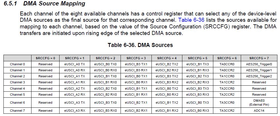
       Channels 6 and 7 on the DMA do not support the SPI implementation on eUSCIB2.  The references for eUSCIB2 that you find in channels 6 and 7 are for the multiple I2C slave addresses that are supported (section 24.3.10 of SLAU356e,

    ).

    (Taken from Datasheet)

      You will need to use DMA channels 4 and 5 as shown in this code example: .

     A similar discussion can be found here around the multiple DMA triggers can be found here:

    Regards,

    Chris

  • Hi Chris,

    Thank you for the clarification and the reference to the discussion...it is really not clear in the manual.

    the only problem is that channel 4,5 are already used by the UART.... which is running at 1Mbit. i cant switch to SPI0, since the HW is already set, so unless there is no other option i'll need to manage the transfer through the SPI ISR.   

    Regards,

    Shai.

  • Shai,
    You may have already looked into this, but would you be able to take advantage of the port mapping and move to UCA0 or UCA1 and to DMA channels 0,1 or 2,3 respectively? I am thinking specifically of pins 3.4-3.7.

    Regards,
    Chris
  • Hi Chris.

    i thought about it but not the only way it can work is if i switch between SPI2 and SPI0 pins (P3.4-7 and P1.4-7) i'm not sure i completely understand the PMAP registers mechanism.... if there is a way to switch the pins, it would solve the problem....any idea?

    regards,

    shai.

  • Shai,
    Pins 1.4 through 1.7 cannot be port mapped. These are fixed with primary function of USCB0 which I interpret what you mean by SPI0. In addition to the USCB0-2 there is also USCA0-2, so on P3.4 through P3.7 you could map USCA0, USCA1, USCA2, in addition to USCB2 which is the default. If you look in the msp432p401.h you will find the various settings for SIMO, SOMI, CLK, etc.

    Unfortunately USCA3 is not available in the port mapping. This would have enabled you to use DMA channels 6 and 7 as you originally proposed. If you can use DMA channels 0 and 1, which are connected to triggers from eUSCI_A0_TX and RX respectively, then you could port map USCA0CLK, USCA0SIMO, USC0SOMI as follows:

    /* Port mapper configuration register */
    const uint8_t port_mapping[] =
    {
    //Port P3:
    PM_NONE, PM_NONE, PM_NONE, PM_NONE, PM_NONE, PMAP_UCA0CLK, PMAP_UCA0SIMO,
    PMAP_UCA0SOMI
    };

    /* Remapping */
    MAP_PMAP_configurePorts((const uint8_t *) port_mapping, PMAP_P3MAP, 3,
    PMAP_DISABLE_RECONFIGURATION);

    MAP_GPIO_setAsPeripheralModuleFunctionOutputPin(GPIO_PORT_P3,
    GPIO_PIN5+GPIO_PIN6+GPIO_PIN7, GPIO_PRIMARY_MODULE_FUNCTION);

    dev.ti.com/.../

    I noticed that you are using the driverLib for some of the APIs and would recommend using for the SPI also:

    dev.ti.com/.../

    /* SPI Master Configuration Parameter */
    const eUSCI_SPI_MasterConfig spiMasterConfig =
    {
    EUSCI_A_SPI_CLOCKSOURCE_SMCLK, // SMCLK Clock Source
    3000000, // SMCLK = DCO = 3MHZ
    500000, // SPICLK = 500khz
    EUSCI_A_SPI_MSB_FIRST, // MSB First
    EUSCI_A_SPI_PHASE_DATA_CHANGED_ONFIRST_CAPTURED_ON_NEXT, // Phase
    EUSCI_A_SPI_CLOCKPOLARITY_INACTIVITY_HIGH, // High polarity
    EUSCI_A_SPI_3PIN // 3Wire SPI Mode
    };

    /* Configuring SPI in 3wire master mode */
    SPI_initMaster(EUSCI_A0_BASE, &spiMasterConfig);

    /* Enable SPI module */
    SPI_enableModule(EUSCI_A0_BASE);

    Hope that helps,
    Chris
  • Hi Chris,

    Thank you for the really good ideas, at the least it got me more familiar with the options of this MSP.
    i was trying to rearrange the functions of the pins, but since the hardware is already set and connected to other boards, i cannot switch pins functions that easily, second thing is that we are using all 3 UARTS and the 64QFN package, which leaves me without any option to map SPI to channel A, the I2C network is connected to the P6.6-7 pins. i cannot make changes to the pins functions, but can only switch between SPIs. that is what i meant when i said that the HW is already set.......
    if there is no way to switch between SPI0 and SPI2. we will need to use the old ISR method, i just wonder if we can make it very short so it will hold 6-8MHz with 48MHz clock (around 50 cycles per byte)...since we are the master here there can be some flexibility in the rate and the continuity of the CLOCK.
    ill still try to see if we can use jumpers on the HW.

    regards,
    shai.

**Attention** This is a public forum