This thread has been locked.

If you have a related question, please click the "Ask a related question" button in the top right corner. The newly created question will be automatically linked to this question.

MSP430FR2633: XT1BYPASS mode question?

Part Number: MSP430FR2633

Hello,

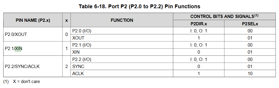
In section 7.1.2 (external oscillator), page 75 of the MSP430FR2633 manual, it states it is possible to use XIN and XOUT as general purpose I/O.  It says it is possible if the appropriate XT1BYPASS mode is selected.  I am trying to simply to set the pins (2.0 and 2.1, XOUT and XIN respectively) as input/output pins with no luck. www.ti.com/.../msp430fr2633.pdf

Using the MSP430 driver lirbary, I called CS_bypassXT1(), but I am not sure if this is sufficient..

Code below:

#include "driverlib.h"

int main(void) {

    WDT_A_hold(WDT_A_BASE);

    CS_bypassXT1();

    GPIO_setAsOutputPin(GPIO_PORT_P2,GPIO_PIN0); //brown p2.2
    GPIO_setOutputHighOnPin(GPIO_PORT_P2,GPIO_PIN0); //brown p2.2
    int i;
    while(1){
        GPIO_toggleOutputOnPin(GPIO_PORT_P2,GPIO_PIN0);
        for( i = 0; i < 20000; i++ );
    }
}

Any help is much appreciated.

Best,

Robert

  • Hello Robert,

    The XT1BYPASS is to use an external clock signal instead of a crystal on those ports, not for using the pins as I/O. It will still be a clock signal.
    You will need to set P2SEL so it will use them as GPIO. It probably is the default configuration.
    Look at page 60 of the manual, and go to the family user guide for better explanation www.ti.com/.../slau445g.pdf

    Hope it helps.
  • The device datasheet states the reset default function is GPIO, but the user guide states XIN/XOUT.
    Try clearing bits 1 and 0 in both P2SEL1 and P2SEL0. That should configure the pins as GPIO.
  • I am fairly new to this so I apologize if this may seem like a simple question. So I tested the following bit of code and was still unable to drive the pin high.

    #include "driverlib.h"
    
    void main(void)
    {
        WDT_A_hold(WDT_A_BASE);             //    WDTCTL = WDTPW | WDTHOLD;  Stop watchdog timer
    
        P2SEL0 &= ~BIT0;
        P2SEL1 &= ~BIT0;
        P2OUT &= ~BIT0;                         // Clear P1.0 output latch for a defined power-on state
        P2DIR |= BIT0;                          // Set P1.0 to output direction
        GPIO_setOutputHighOnPin(GPIO_PORT_P2,GPIO_PIN0);
    
        while (1);
    }

    From the MSP430FR2633 datasheet I extracted this table from page 60.

    As mentioned before, P2SELx has to be set to 0 which I believe I have done correctly using:

        P2SEL0 &= ~BIT0;
        P2SEL1 &= ~BIT0;

    In the above code, the x in the table is replaced by whichever pin I am attempting to set (which does not seem to be the case with P2DIR.x)

    The remainder of the code I pulled from a tutorial.  Not quite sure what "Clear P1.0 output latch for a defined power-on state" exactly means or if it is necessary.

    Regarding P2DIR.x from the datasheet, I tried setting P2DIR.0 |= BIT0; (equivalent to P2DIR.0 = 0x01) but this left me with a compilation error.  Could someone please explain how P2DIR.x translates to code.  An example showing all 3 pins (P2.0, P2.1, P2.2) driven both high and low would be extremely helpful, and would let me see how the table has to be read and coded.

    Some simpler code that does not work:

        P2SEL0 = 0; //&= ~BIT0;
        P2SEL1 = 0; //&= ~BIT0;
        P2DIR |= (BIT0 | BIT1);                   // set P1DIR with P0 and P6 to high (1)
    
        int i;
        for (;;) {
            P2OUT ^= (BIT0 | BIT1);               // toggle the P0 and P6 of P1OUT with 1 and 0
            for( i = 0; i < 20000; i++ );
        }
    

    Much appreciated.

    Best,

    Robert

  • As for setting P2DIR.0, check how it was defined and you'll probably find it's not addressable like that. You should find the struct for the bits of P2 and then you can modify them like that.

    Check the User Guide, section 7 has the I/O.
    PxSEL select modules
    PxDIR sets IN/OUT
    PxOUT sets the output

    That last code should work, how are you verifying it's /it's not working?
  • I will review the user guide. I am verifying the outputs with a scope.

    Best,
    Robert
  • Since you have no code inside the for(i=0....), it might be optimized and eliminated.

    Try something like

    P2SEL0 = 0;                               //Set PSEL to GPIO
    P2SEL1 = 0;
    P2DIR |= (BIT0 | BIT1);                   // set P1DIR with Bits 0 and 1 to high (1)
    P2OUT = 0;
     
    for (;;) {
        P2OUT ^= (BIT0 | BIT1);               // toggle the Bits 0 and 1 of P1OUT
        __no_operation();                  // adds one cycle NOP
    }
    Also make sure it's running, try debugging and step the code. It might need more initialization and it could not arrive to where you expect it to be.
  • PM5CTL0 &= ~LOCKLPM5; // Disable the GPIO power-on default high-impedance mode

    Adding this to the top of your code fixed it.. Thank you so much for your help. Took way to long to figure that one out.

    Best,
    Robert

**Attention** This is a public forum