This thread has been locked.

If you have a related question, please click the "Ask a related question" button in the top right corner. The newly created question will be automatically linked to this question.

My LaunchPad Satellite Board

Other Parts Discussed in Thread: MSP430G2231

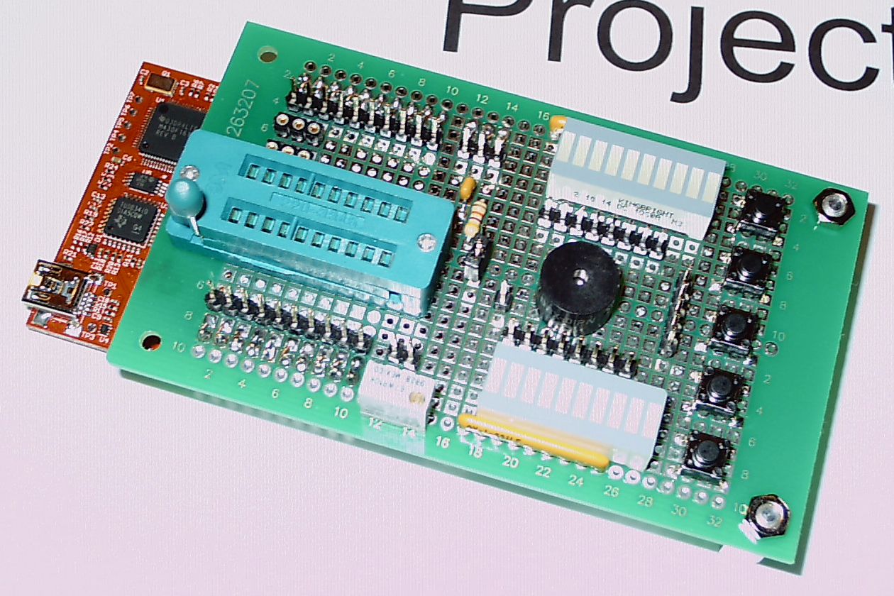
I just finished building an expansion board for my LaunchPad.   I"ve tried insterting a picture of it in this post.  If this doesn't work, see my user profile's Files section.

Description.  The expansion board has the following features:  20-pin ZIF socket, sockets for high speed crystal and associated caps, 5 pushbuttons (active low), one of which can be used as a reset button via jumper, two banks of 8 LEDs each (active high), multi-turn 10K pot, piezo tone transducer.  All connections (other than common grounds) are via headers and jumper cables.

Building Method.  Thru-hole plated perf board (Jameco 263207/PCB-463) and point-to-point wiring.  The two outboard legs are 9/16ths hex standoffs with an additional nylon washer.

Notes.  The MSP430 chip can be put either on the LaunchPad or in the zif socket.  The pull-up resistor and pull-down cap for S2/P1.3 on the LaunchPad were removed.  If a 32768 Hz clock crystal is to be used, it and the MSP430 should be mounted on the LaunchPad and resistors R28 and R29 removed.  (I plan on having two LaunchPads, one without the clock crystal and one with it installed.)  J6 as well as J1 and J2 were brought up to the satellite board.  Only 8 of the 10 LEDs in the bar graph displays are used.  One display is bright red (Mouser 604-DC10SRWA) with 330 ohm dropping resistors, the other is green (Mouser 604-DC10GWA) with 220 ohm dropping resistors.  (I used Bourns resistor networks.)  The MSP430 pins for the pushbuttons must use internal pull-up resistors.  The connections to Pins 20 and 19 on the ZIF socket are criss-crossed to and from the crystal/cap sockets so the ground connections on these are in the middle.

Comments.  I did not draw a schematic for this project, as it is so straight-forward.  I expect this board to be useful as a programming platform for projects that don't use a clock crystal on XIN/XOUT, and it will also allow me to try out more programming exercises (e.g., multiple button input, tone production, A-to-D conversions, lots of pretty flashing LEDs, etc.) than the LaunchPad itself.  The TI developers were wise in designing the LaunchPad headers to allow such expansion boards.

Cheers, Andy


  • Nicely done!  That's a good use of the launchpad's IO header resources and of a 0.1" grid array board.

    I think it would have been good to have some more peripheral resources like LEDs / switches / drivers / receivers right on the MSP430 eval board like the launchpad even if they were unpopulated but just available for optional stuffing and optional connection sort of as you've done in your expansion board, but as you've shown it isn't too terribly difficult to add some extra bells and whistles using $20 or whatever of added parts and some soldering work.

    I'll be making something with some optocoupler inputs, mechanical and SSR relay outputs, and a rotary encoder soon, though that's for a particular use project versus a prototyping board.

    Congratulations on the nice little expansion board.

    PS watch out for the maximum source/sink current rating of all combined MSP outputs when driving a bunch of regular sensitivity LEDs, as well as the power dissipation rating of the input regulator depending on what power its handling ability is and its input supply voltage.  Probably not a problem with 5V USB in and 3.3V out or whatever.  A linear regulator drop out power gets a bit much in general at higher supply voltages like 9V or 12V if you're driving a couple LEDs and such at 3.3V VCC output if you're using such a regulator instead of the USB power sometimes.


  • Very cool board! Do you take the power from the 10 pin headers on the side? or also have a connection for the 3 pin header on the launchpad?

    Also, since you mentioned the power consumption issue, it gave me another idea for the proposal I'm writing up. Hopefully anyone who makes an expansion board for the device will post pictures! This really helps, at least with idea's.

    Great job on the board.

    -NJC

    ______________________________

    http://msp430launchpad.blogspot.com

  • Nice job.

    To follow the LED supply considerations, I might add, that I use low-driven LEDs in my own projects.

    This way, their power is taken from the 5V supply rtather than the (50mA only) low-drop 3.3V regulator.
    Also, it allows for driving blue or white LEDs where the MSP output voltage might not be high enough.
    As an additon, blinking the LEDs does not affect the performance of ADC or DAC, while sourcing the LEDs through the MSP pins and therefore the MSPs VCC does.

    It does, however, only work as long as the difference between the LEDs supply voltage and the MSP supply voltage isn't higher than the on-voltage of the LEDs (plus 0.2V for the port pin clamp diode voltage). Else the LEDs begin to glow even in off-state.
    The 1.7V between 5V and 3.3V are fine.

    Currently, I'm working on an experimental board for the 5438. It will feature analog input for voltage/current/current loop (software selectable), capacitive touchpads, LCD support (external module with parallel or SPI port)rotary encoder, voltage/current output, 3-phase energy meter, external RTC etc. It won't be for general experiments, as all the circuitry is intended for actual projects, yet it will allow developing all the software modules and testing the hardware components before the hardware design for the actual projects is made.

  • Thanks for all your comments, folks. 

    I do bring the three pin header up to the expansion board and connect the two ground and one Vcc pin to the MSP430 ground and power pins, so I could (at least in principle) power everything from the three pin headers if I removed the satellite board from the LaunchPad. 

    With the LED dropping resistors I used the current draw for each LED is calculated to be 4 to 5 ma, pretty much at the suggested per-pin limit, I think.  I'm running on thin ice here, hoping that the port maximum will be exceeded for only short periods of time, or that DIP devices can handle the overload due to their larger mass.  Perhaps I could adapt the MSP430G2231 LaunchPad demo program to tell me just how hot the chip gets if I drive all 8 LEDs on a port? 

    The only real MSP430 project I've built so far runs on a button cell, but I have purchased some 3.3v LDO 100 ma regulators and some 1A linear regulators in anticipation of future projects.  I know all about heating regulators up.  A year ago I built a homebrew 75 meter single sideband transceiver that used a digitially synthesized variable frequency oscillator based on a ham kit called the DDS-60.  The board had a SMT 5v regulator for the Analog Devices synthesizer chip but most of the radio's circuitry used 13.8v.  Boy, did that regulator get hot!  I had to add a heat-sinked 8v regulator to feed the 5v board to keep things cool. 

    Generally, as a hobbyist I reserve the right to ignore good engineering practice when I feel impatient or lazy.  The only price I pay is about $2.50 retail for a new MCU chip, and no one else needs to know.  I'm very glad I don't have a supervisor keeping tabs on what I do. 

    Cheers.


  • Andrew Palm said:
    pretty much at the suggested per-pin limit

    Actually there isn't such a thing as a per-pin-limit or per-port-limit. There's only a maximum current at which a specific maximum voltage drop is guaranteed. There is, of course, a saturation current, but it is in the range of 20-25mA per pin (I didn't test and the datasheet doesn't tell).

    There is, however, a maximum power dissipation, which includes the power spent on the output pins (voltage drop*current). For a voltage drop of 0.6V @15mA (MSP5438), it is 90mW per pin, and since the MSP5438 can bear up to ~1W without heat sink (55K/W junction/ambient) and up to 6W with perfect cooling (8.9K/W junction/case), you can source/sink up to 150mA/1A total through the port pins (evenly distributed with 15mA/pin). With more pins and less mA/pin even more.

    I don't know the actual limits of the 2231, bu tI don't think that your 5mA/LED will come near the limits even with all LEDs on.

    Andrew Palm said:
    The only price I pay is about $2.50 retail for a new MCU chip

    If it is a DIP chip and in a socket, that's fine. If it's a 100-pin PQFP or even a BG chip soldered onto the board, the price of the chip is void compared to the efforts to replace it. If you can replace it at all without damaging the board beyond repair.

    Andrew Palm said:
    I'm very glad I don't have a supervisor keeping tabs on what I do. 

    Lucky you!

  • Thanks for clearing that up for me, JMG.  I ran a little test with 10 LEDs on and the chip remained cool.  From what you say, I can see why. 

    After retirement I worked for a little over a year as a pager repair tech on Motorola 1990's vintage pagers.  I did some SMT parts removal, but mostly just SMT trim caps.  I tried a few high-pin-count ICs and it could be a real mess, as you point out.  Since I no longer have access to desoldering tools like hot tweezers, removing the P1.3 pull-up resistor and pull-down cap on the LaunchPad was a challenge, especially since they seem to be the smallest discrete SMT component sizes I've ever seen.  I also missed having a microscope. 

    Thanks again. 

  • andrew - very cool!  i'm looking forward to see it running some code.

  • Andrew Palm said:
    I tried a few high-pin-count ICs and it could be a real mess

    I usually cut the pins directly at the case. Then I can wipe them away with a soldering iron. It destroys teh chip, but if you don't cut into the board wires, you can start over with a new one. I already did this many years ago when removing defective DIP RAM or I/O chips on the C64. Cut the pins and then pull them one by one.
    Bot these shrink-.small-outline packages are a real mess to solder.

    Andrew Palm said:
    they seem to be the smallest discrete SMT component sizes I've ever seen

    Indeed, there are some parts you can't even see or at least classify with bare eyes. Yet TI usually uses 0805 size, which is quite large. We once got a delivery of 0403 or even smaller capacitors. We couldn't even tell which sides were the ones to solder (far away from actually doing so). Despite of the nice x3 spectacles we got for SMD work.
    Then one day someone dropped the box. Since then all those nice tiny capacitors are just ceramic sand. Good for a nice (and expensive) hourglass.

  • Adrian, you asked to see the board running code, so here it is.  The flash washed out the LEDs that were on.  Also, the jumper to the tone transducer is disconnected as after a while the sound got annoying.  The code, for what it is worth, is below.  I used an MSP430G2231.

    The LEDs display the lower 8 bits of a 16-bit pseudo-random sequence (3 taps for maximum length).  I use the WDT in the background to generate a square wave of about 488 Hz.  This is turned off and on by changing the port pin direction bit.  It is turned on when LED/Bit 7 is lit.  The ADC code is very crude as I just copied the one-shot example from Davies' book into the program.  The ADC reading is used to change the Timer A interval which determines how frequently the bit sequence is changed.  Turning the pot adjustment screw CW slows the display.  (If the ADC is turned too far CCW the program hangs up, as the Timer A interval is too short.  I could have fixed this, but haven't bothered.)  I didn't put in any pushbutton testing, as I ran out of general i/o pins.

    Cheers, Andy

     //-------------------------------------------------------------------------
    //  cProtoboardTest3.c - Pseudorandom sequence with sound and ADC used to
    //                       vary display speed.
    //
    //  Andy Palm
    //  2010.08.05
    //-------------------------------------------------------------------------
    #include <msp430g2231.h>
    #include <stdint.h>

    // Helpful general defines
    #define clear_bit( reg, bitmask )  ((reg) &= ~(bitmask))
    #define set_bit( reg, bitmask )    ((reg) |= (bitmask))
    #define test_bit( reg, bitmask )   ((reg) & (bitmask))
    #define toggle_bit( reg, bitmask ) ((reg) ^= (bitmask))

    // Global variables
      uint16_t  pattern;                    // Bit pattern shift register
      uint16_t  tap3, tap12, tap14;         // Tap values

    //-------------------------------------------------------------------------
    //  Interrupt service routine for WDT
    //  Generates approx 488 Hz square wave on P2.7
    #pragma vector = WDT_VECTOR
    __interrupt void WDT_ISR(void)
    {
      toggle_bit(P2OUT, BIT7);              // Toggle output to tone transducer

    //-------------------------------------------------------------------------

    //  Interrupt service routine for Timer A Channel 0
    #pragma vector = TIMERA0_VECTOR
    __interrupt void TA0_ISR(void)
    {
      __low_power_mode_off_on_exit();

    //-------------------------------------------------------------------------
    void main(void)
    {
    // Stop watchdog timer
      WDTCTL = WDTPW + WDTHOLD;

    // Set up system clocks, here DCO at 1 MHz
      BCSCTL1 = CALBC1_1MHZ;                // Set DCO range
      DCOCTL = CALDCO_1MHZ;                 // Set DCO step and modulation
      BCSCTL2 = DIVS_1;                     // SMCLK = DCO/2
      BCSCTL3 = LFXT1S_2;                   // Select ACLK from VLO

    // Set up watchdog timer in interval mode for generating tone of 488 Hz
      WDTCTL = WDT_MDLY_0_5;                // From SMCLK, period 512
      IE1 = WDTIE;                          // Enable WDT interrupt

    // Configure port P2 for digital i/o when external xtal not used
      P2SEL = 0;                            // Port 2 digital i/o
      P2OUT = 0;                            // Ground outputs
      P2DIR = BIT6;                         // P2.6 pin as output
     
    // Configure port P1 
      P1OUT = 0;                            // LEDs off
      P1DIR = 0xFF;                         // LED pins set as outputs

    // Timer A in count up mode, clock SMCLK/2, clear timer
      TACCR0 = 62499;                       // Timer count for 1 sec
      TACCTL0 = CCIE;                       // Enable interrupt on Compare 0
      TACTL = MC_1|ID_3|TASSEL_2|TACLR;     // Set up Timer A

    // ADC Vcc, Vss refs, sample for 4 cycles, int ref off, ADC on no ints
      ADC10CTL0 = SREF_0|ADC10SHT_0|ADC10ON;
    // Input channel 7, trigger w/ADC10SC bit, no clk div, int ADC clk,
    // single channel, single conversions
      ADC10CTL1 = INCH_7|SHS_0|ADC10DIV_0|ADC10SSEL_0|CONSEQ_0;
      ADC10AE0 = BIT7;                      // Analog input on Ch. 7
      set_bit(ADC10CTL0, ENC);              // Enable conversions

    // Use initial ADC reading to seed random sequence
      set_bit(ADC10CTL0, ADC10SC);          // Start ADC conversion
      while(test_bit(ADC10CTL0, ADC10BUSY)); // Wait for conversion finish
      pattern = ADC10MEM;

      __enable_interrupt();                 // Enable interrupts
     
      for(;;)                               // Wait for interrupt
      {
        __low_power_mode_0();               // Enter low power mode LPM0

        set_bit(ADC10CTL0, ADC10SC);        // Start ADC conversion
        while(test_bit(ADC10CTL0, ADC10BUSY)); // Wait for conversion finish
        TACCR0 = ADC10MEM << 6;             // Update Timer A count limit
       
        P1OUT = (uint8_t) (pattern & 0x7F); // Display bits 0 to 6
        if(test_bit(pattern, BIT7))         // Display bit 7 on P2.6
        {                                   // Play tone if bit 7 is set
          set_bit(P2OUT, BIT6);
          set_bit(P2DIR, BIT7);
        }
        else
        {
          clear_bit(P2OUT, BIT6);
          clear_bit(P2DIR, BIT7);
        }

        tap3  = (pattern & (1<<3)) >> 3;    // Get tap values and shift to bit 0
        tap12 = (pattern & (1<<12)) >> 12;
        tap14 = (pattern & (1<<14)) >> 14;
       
        pattern <<= 1;                      // Shift pattern left
        pattern |= (tap3 ^ tap12) ^ tap14;  // Put mod 2 sum of taps into bit 0

      }
     }


  • One small addendum.  I realized that I can use one LaunchPad with the satellite board for either situation--when using a clock crystal or not using one. 

    I'll solder the supplied clock crystal to the LaunchPad and remove the jumpers to the header for those two pins as recommended in the User Guide.  Then if I develop a project requiring a clock crystal, I'll put the MSP430 chip in the LaunchPad socket.  (There is just enough clearance.)  If I don't need a clock crystal, I can put the chip in the satellite board socket and the P2.6 and P2.7 pins will be available for general i/o use, as there will be no connection of them to the crystal.

    Cheers, Andy

**Attention** This is a public forum