This thread has been locked.

If you have a related question, please click the "Ask a related question" button in the top right corner. The newly created question will be automatically linked to this question.

MSP430FR5889: Problem in reading ADC in FR Series having ESI module.

Part Number: MSP430FR5889
Other Parts Discussed in Thread: MSP-EXP430FR6989

Dear Team,

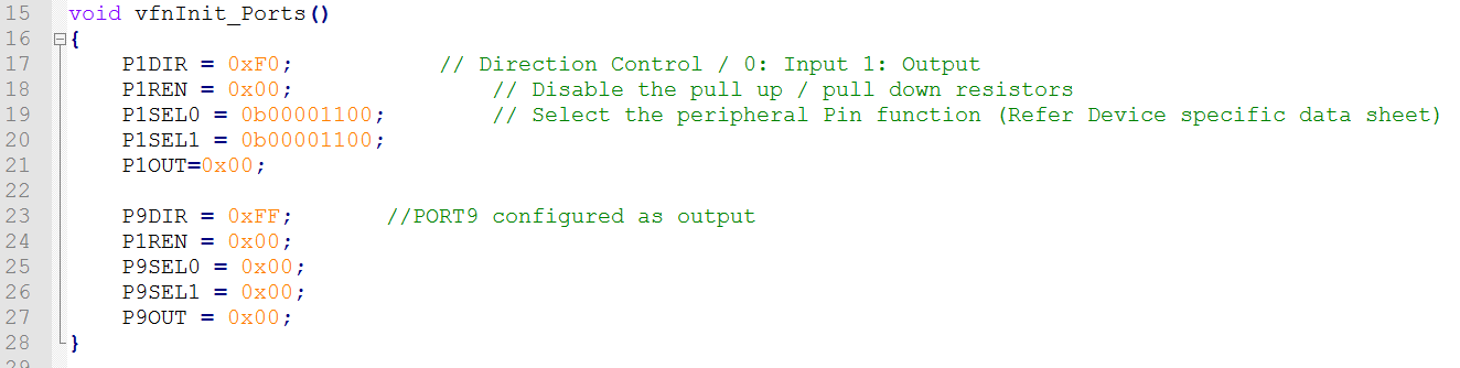
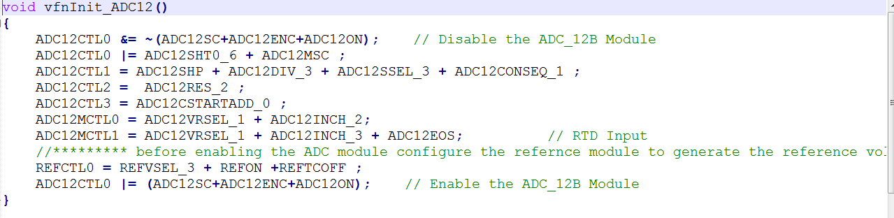
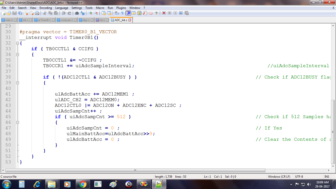
We are facing issue in reading ADC channel A3 (P1.3) in MSP430FR5889 microcontroller. The raw ADC value is varying continuously. But When we changed the P9 output port value to 0x00(i.e P9OUT = 0x00) the reading looks stable. We later noticed that Port 9 is multiplexed with ESI module pins. We have also checked in the debugger the ESI Module register which is to be disabled. 

Kindly help us to solve the issue. How would loading 0x00 to Port 9 stabilized the ADC value. ? 

  • Vijeth,

    Would you be capable of sharing port, ESI, and ADC initialization code as well as screenshots of the issue? The ESI should not matter on port 9 if functionality has not been selected by the P9SEL registers. At any rate it is recommended that unused pins are driven as outputs low.

    Regards,
    Ryan
  • Dear Ryan,

    Kindly find the screen shots of the Port settings, ADC Settings, ESI we are not configuring . Default value is retained. We are using 8 Mhz crystal for HF XTAL pins.

    MCLK = 8 Mhz

    SMCLK = 8 Mhz

    ADC Clock = 2 Mhz

    The input voltage for A3 which is configured for ADCMEM1 is 0V. Still the raw adc counts are very high.

  • Hi Vijeth,

    Are you disabling the GPIO power-on default high-impedance mode to activate previously configured port settings (PM5CTL0 &= ~LOCKLPM5;)?
    Similar behavior is not found on P1.2? And it occurs on all conversions, not just the first few? Does the issue persist if you only sample from A3 in single-channel mode? Separate from the issue at hand, why aren't you using TimerB as the ADC12 sample and hold source select? in place of a software ADC12SC?

    Regards,
    Ryan
  • Sir,

    Are you disabling the GPIO power-on default high-impedance mode to activate previously configured port settings (PM5CTL0 &= ~LOCKLPM5;)?
    --------------------------------------------------------------------------------------------------------------------------------------------------------------------Century:Yes.As always ON POWER ON all ports are on high impedance mode AND programmed as needed by the project afterwards.
    _____________________________________________________________________________________________
    Similar behavior is not found on P1.2? And it occurs on all conversions, not just the first few?
    Century:Yes, on P1.2,&P1.3
    ____________________________________________________________________________________________
    Does the issue persist if you only sample from A3 in single-channel mode?
    ---------------------------------------------------------------------------------------------------------------------------------------------------------------
    Century:YES.
    _______________________________________________________________________________________
    Separate from the issue at hand, why aren't you using Timer B as the ADC12 sample and hold source select? in place of a software ADC12SC?
    ________________________________________________________________________________________________

    Century:Timer B is used for compare & capture for ADC SAMPLE TIME GENERATION,(WE capture the mains frequency, average and generate ADC sample times to enhance NORMAL MODE REJECTION).

    The real issue is port 1 gets disturbed when we write on PORT 9.

    As written earlier, PORT1 Functions NORMALLY if port 9 is not used

    Can we find any solution.

    Regards
    VTC
  • Can you please demonstrate the behavior with slight modifications to an ADC C example provided by TI?  This will help start an internal investigation, as it stands I could not reproduce the error with the following code (not optimized for your application):

    #include <msp430.h>
    
    volatile unsigned int result = 0;
    
    int main(void)
    {
      WDTCTL = WDTPW | WDTHOLD;                 // Stop WDT
    
      // Configure GPIO
      P1OUT &= ~BIT0;                           // Clear LED to start
      P1DIR |= BIT0;                            // Set P1.0/LED to output
      P1SEL1 |= BIT2 | BIT3;                    // Configure ADC inputs A2 and A3
      P1SEL0 |= BIT2 | BIT3;
    
      P9DIR = 0xFF;
      P1REN = 0x00;
      P9SEL0 = 0x00;
      P9SEL1 = 0x00;
      P9OUT = 0x00;
    
      // Disable the GPIO power-on default high-impedance mode to activate
      // previously configured port settings
      PM5CTL0 &= ~LOCKLPM5;
    
      // By default, REFMSTR=1 => REFCTL is used to configure the internal reference
      while(REFCTL0 & REFGENBUSY);              // If ref generator busy, WAIT
      REFCTL0 |= REFVSEL_0 | REFON;             // Select internal ref = 1.2V
                                                // Internal Reference ON
    
      // Configure ADC12
      ADC12CTL0 = ADC12SHT0_6 | ADC12ON | ADC12MSC;       // Sampling time, ADC12 on
      ADC12CTL1 = ADC12SHP | ADC12DIV_3 | ADC12CONSEQ_1;                     // Use sampling timer
      ADC12CTL2 |= ADC12RES_2;                  // 12-bit conversion results
      ADC12MCTL0 |= ADC12INCH_2 | ADC12VRSEL_1;     // Channel2 ADC input select; Vref=AVCC
      ADC12MCTL1 |= ADC12INCH_3 | ADC12VRSEL_1 | ADC12EOS;     // Channel2 ADC input select; Vref=AVCC
      ADC12IER0 |= ADC12IE0;                    // Enable ADC conv complete interrupt
    
      while(!(REFCTL0 & REFGENRDY));            // Wait for reference generator
                                                // to settle
    
      while (1)
      {
        __delay_cycles(5000);
        ADC12CTL0 |= ADC12ENC | ADC12SC;        // Start sampling/conversion
    
        __bis_SR_register(LPM0_bits + GIE);     // LPM0, ADC12_ISR will force exit
        __no_operation();                       // For debugger
      }
    }
    
    #if defined(__TI_COMPILER_VERSION__) || defined(__IAR_SYSTEMS_ICC__)
    #pragma vector = ADC12_VECTOR
    __interrupt void ADC12_ISR(void)
    #elif defined(__GNUC__)
    void __attribute__ ((interrupt(ADC12_VECTOR))) ADC12_ISR (void)
    #else
    #error Compiler not supported!
    #endif
    {
      switch(__even_in_range(ADC12IV, ADC12IV_ADC12RDYIFG))
      {
        case ADC12IV_NONE:        break;        // Vector  0:  No interrupt
        case ADC12IV_ADC12OVIFG:  break;        // Vector  2:  ADC12MEMx Overflow
        case ADC12IV_ADC12TOVIFG: break;        // Vector  4:  Conversion time overflow
        case ADC12IV_ADC12HIIFG:  break;        // Vector  6:  ADC12BHI
        case ADC12IV_ADC12LOIFG:  break;        // Vector  8:  ADC12BLO
        case ADC12IV_ADC12INIFG:  break;        // Vector 10:  ADC12BIN
        case ADC12IV_ADC12IFG0:                 // Vector 12:  ADC12MEM0 Interrupt
            result = ADC12MEM0;                 // read out the result register
          __bic_SR_register_on_exit(LPM0_bits); // Exit active CPU
          break;                                // Clear CPUOFF bit from 0(SR)
        case ADC12IV_ADC12IFG1:   break;        // Vector 14:  ADC12MEM1
        case ADC12IV_ADC12IFG2:   break;        // Vector 16:  ADC12MEM2
        case ADC12IV_ADC12IFG3:   break;        // Vector 18:  ADC12MEM3
        case ADC12IV_ADC12IFG4:   break;        // Vector 20:  ADC12MEM4
        case ADC12IV_ADC12IFG5:   break;        // Vector 22:  ADC12MEM5
        case ADC12IV_ADC12IFG6:   break;        // Vector 24:  ADC12MEM6
        case ADC12IV_ADC12IFG7:   break;        // Vector 26:  ADC12MEM7
        case ADC12IV_ADC12IFG8:   break;        // Vector 28:  ADC12MEM8
        case ADC12IV_ADC12IFG9:   break;        // Vector 30:  ADC12MEM9
        case ADC12IV_ADC12IFG10:  break;        // Vector 32:  ADC12MEM10
        case ADC12IV_ADC12IFG11:  break;        // Vector 34:  ADC12MEM11
        case ADC12IV_ADC12IFG12:  break;        // Vector 36:  ADC12MEM12
        case ADC12IV_ADC12IFG13:  break;        // Vector 38:  ADC12MEM13
        case ADC12IV_ADC12IFG14:  break;        // Vector 40:  ADC12MEM14
        case ADC12IV_ADC12IFG15:  break;        // Vector 42:  ADC12MEM15
        case ADC12IV_ADC12IFG16:  break;        // Vector 44:  ADC12MEM16
        case ADC12IV_ADC12IFG17:  break;        // Vector 46:  ADC12MEM17
        case ADC12IV_ADC12IFG18:  break;        // Vector 48:  ADC12MEM18
        case ADC12IV_ADC12IFG19:  break;        // Vector 50:  ADC12MEM19
        case ADC12IV_ADC12IFG20:  break;        // Vector 52:  ADC12MEM20
        case ADC12IV_ADC12IFG21:  break;        // Vector 54:  ADC12MEM21
        case ADC12IV_ADC12IFG22:  break;        // Vector 56:  ADC12MEM22
        case ADC12IV_ADC12IFG23:  break;        // Vector 58:  ADC12MEM23
        case ADC12IV_ADC12IFG24:  break;        // Vector 60:  ADC12MEM24
        case ADC12IV_ADC12IFG25:  break;        // Vector 62:  ADC12MEM25
        case ADC12IV_ADC12IFG26:  break;        // Vector 64:  ADC12MEM26
        case ADC12IV_ADC12IFG27:  break;        // Vector 66:  ADC12MEM27
        case ADC12IV_ADC12IFG28:  break;        // Vector 68:  ADC12MEM28
        case ADC12IV_ADC12IFG29:  break;        // Vector 70:  ADC12MEM29
        case ADC12IV_ADC12IFG30:  break;        // Vector 72:  ADC12MEM30
        case ADC12IV_ADC12IFG31:  break;        // Vector 74:  ADC12MEM31
        case ADC12IV_ADC12RDYIFG: break;        // Vector 76:  ADC12RDY
        default: break;
      }
    }

    Regards, Ryan

  • Dear Ryan, 

    The above code works because P9OUT = 0x00 , Please try writing some values to the Port 9 and read ADC A2 and A3.  

  • I set P9OUT = 0xFF and the A2/A3 readings were still as expected. This could indicate an issue with the PCB layout. I should mention that this is using a MSP-EXP430FR6989, a device whose architecture the MSP430FR5889 is based from.

    Regards,
    Ryan
  •  Dear Ryan,

    In progress to resolve our issue Kindly find attached the oscilloscope output checked at microcontroller pin A2 with connecting adc input and without connecting adc input.

    some pulse of 2.855Khz frequency is generated at this PIN. Also find attached the Source code for the application.

     Test ADC.zip 

  • Are these oscilloscope findings independent of P9OUT? The test ADC code can be further reduced to show only the error at hand but the screenshots seems to further indicate a hardware issue. Are you able to share schematics and layout images?

    Regards,
    Ryan
  • Dear Ryan,

    No, We are using P9OUT in this project as seven segment display output.

    Yes the code can be reduced but since we wanted to debug in the free run mode we have maintained the display part in the code.

    Can you share us your E-mail id so that we can send our project schematic and layout details.(Company terms to maintain confidentiality)

    NOTE: Even if there is no ADC input to the pin , it is generating pulse as you can see in the above image.

  • Dear Ryan,

    NOTE: We get stable pulse when we load with 10K resistor of around 2.8KHz frequency at A2 input PIN.

    We also use in this code capture input TB0.3 to capture mains frequency (around 50 Hz = 20 ms).

    We divide this time by 64 to get the adc sample interval and generate compare interrupt TB0CCTL1 at this rate (i.e 20ms/64 = 312
    us(3.2KHz)).

    We are also not using low frequency crystal . PINS are left open

    We have mailed the necessary documents. 

  • I've responded to your message, perhaps we can carry on the conversation from there.

    Regards,
    Ryan

**Attention** This is a public forum