This thread has been locked.

If you have a related question, please click the "Ask a related question" button in the top right corner. The newly created question will be automatically linked to this question.

CCS/MSP430FR5739: Issue using DMA + ADC10

Part Number: MSP430FR5739
Other Parts Discussed in Thread: MSP430WARE

Tool/software: Code Composer Studio

Hi, I'm using the ADC10 in repeated-single channel mode for convert two channels. I use the ADCIFG as trigger for DMA0, which is configured to get 8 ADC readings from ADC10MEM0 and transfering to a buffer using DMA0SZ=8. I start conversion for a channel (e.g A0) five times and then read another channel (e.g. A1). The problem I found is that the buffer contains two readings from previous conversions, for example:

t=1, A0_buffer=[490, 491, 490, 491, 489, 490, 490, 491]

t=2, A0_buffer=[490, 491, 480, 481, 482, 480, 480, 481]

t=3, A0_buffer=[480, 481, 490, 491, 489, 490, 490, 491]

t=4, A0_buffer=[490, 491, 480, 481, 481, 480, 480, 481]

t=5, A0_buffer=[480, 481, 490, 491, 489, 490, 490, 491]

t=5, A1_buffer=[490, 491, 690, 691, 689, 690, 690, 691]

t=6, A0_buffer=[690, 691, 490, 491, 489, 490, 490, 491]

This example supposes that at t1, t3, t5 and t6, reading at channel A0 are around 490, and for t2 and t4, readings for channel A0 are ~480. Channel A1 is supposed to be at ~690.

These are the steps I am following to do this:

1. Configure DMA (destination address),

2. Configure ADC (channel),

3. Enable DMA

4. Start ADC conversions.

5. When DMA interrupt is active, disable ADC

After doing some debugging I found that the first time I run the program (t1) in step 3, DMA0SZ=8 then in step 4, DMA0SZ remains the same. In the second cycle (t2), DMA0SZ=8 in step 3 but after enabling DMA with DMAEN bit and steping to the next line, DMA0SZ changes to 6. This explains why two readings are wrong in the final buffer.

Any hint on this issue?

  • Hello,

    Thank you for providing a detailed summary of the behavior that you're seeing. With this in mind, it would be very helpful if you could share your code. Since the results in the buffer at t1 seem to be ok and the results at t2 seem to be wrong, I suspect that maybe an initial setting for the ADC or DMA is configured properly (e.g. code in main()) but not for the next iterations (code in an ISR and/or while() loop). Sharing your code will help us know more details such as single versus block transfers, ADC10IFG0 flag set by hardware or software, etc.

    For the second cycle, you mention that DMA0SZ changes to 6 when you reach step 4. For this step, the ADC conversions get started. If DMA0SZ changes to 6 before the ADC is started, this means that two transfers have already occurred. Thus, I suspect that the ADC may be still running and is already triggering the DMA.

    Let me also point out that there are several ADC and DMA errata for this device that may be influencing or causing this behavior. In the meantime, I would suggest looking at the 'MSP430FR57xx_adc10_15.c' code example. You may have already done that, but it's a good reference that I wanted to mention.

    Regards,

    James

    MSP Customer Applications
  • Hi James, thanks for your response. I will reduce the code to minimum that replicates the issue, meanwhile, I will give you some details. This is part of the code:

    void adc_start_conversion()
    {
    while (ADC10CTL1 & ADC10BUSY);
    __bis_SR_register(GIE);
    ADC10CTL1 |= ADC10CONSEQ_2;
    ADC10CTL0 |= ADC10ENC + ADC10SC;
    }
    
    ...
    
    if (var == TEMP) {
        dma_set_dest(adc_vars.temp_buff_samples); // step 1
        adc_set_channel(ADC10INCH_2); // step 2
    } else {
        dma_set_dest(adc_vars.batt_buff_samples); // step 1
        adc_set_channel(ADC10INCH_0); // step 2
    }
    dma_enable(); // DMA0CTL |= DMAEN + DMAIE, step 3
    adc_start_conversion(); // step 4
    
    ...


    I set two breakpoints, one at dma_enable() and another at adc_start_conversion(). These is the state of registers at each breakpoint in cycle 1 (t1) and cycle 2 (t2):

    Cycle 1: (works)

    Breakpoint 1 (before dma_enable):
    ADC10CTL0 0x0290 ADC10 Control 0 [Memory Mapped]
    ADC10CTL1 0x0200 ADC10 Control 1 [Memory Mapped]
    ADC10CTL2 0x0010 ADC10 Control 2 [Memory Mapped]
    ADC10LO 0x0000 ADC10 Window Comparator High Threshold [Memory Mapped]
    ADC10HI 0x03FF ADC10 Window Comparator High Threshold [Memory Mapped]
    ADC10MCTL0 0x0012 ADC10 Memory Control 0 [Memory Mapped]
    ADC10MEM0 0x01FE ADC10 Conversion Memory 0 [Memory Mapped]
    ADC10IE 0x0000 ADC10 Interrupt Enable [Memory Mapped]
    ADC10IFG 0x0000 ADC10 Interrupt Flag [Memory Mapped]
    ADC10IV 0x0000 ADC10 Interrupt Vector Word [Memory Mapped]
    DMACTL0 0x001A DMA Module Control 0 [Memory Mapped]
    DMACTL1 0x0000 DMA Module Control 1 [Memory Mapped]
    DMACTL2 0x0000 DMA Module Control 2 [Memory Mapped]
    DMACTL3 0x0000 DMA Module Control 3 [Memory Mapped]
    DMACTL4 0x0000 DMA Module Control 4 [Memory Mapped]
    DMAIV 0x0000 DMA Interrupt Vector Word [Memory Mapped]
    DMA0CTL 0x0C24 DMA Channel 0 Control [Memory Mapped]
    DMA0SA 0x00000712 DMA Channel 0 Source Address [Memory Mapped]
    DMA0DA 0x00001D74 DMA Channel 0 Destination Address [Memory Mapped]
    DMA0SZ 0x0008 DMA Channel 0 Transfer Size [Memory Mapped]
    DMA1CTL 0x0000 DMA Channel 1 Control [Memory Mapped]
    DMA1SA 0x00008384 DMA Channel 1 Source Address [Memory Mapped]
    DMA1DA 0x0002846F DMA Channel 1 Destination Address [Memory Mapped]
    DMA1SZ 0xBE96 DMA Channel 1 Transfer Size [Memory Mapped]
    DMA2CTL 0x0000 DMA Channel 2 Control [Memory Mapped]
    DMA2SA 0x00018828 DMA Channel 2 Source Address [Memory Mapped]
    DMA2DA 0x00003180 DMA Channel 2 Destination Address [Memory Mapped]
    DMA2SZ 0x521F DMA Channel 2 Transfer Size [Memory Mapped]
    -----
    Breakpoint 2 (after dma_enable):
    ADC10CTL0 0x0290 ADC10 Control 0 [Memory Mapped]
    ADC10CTL1 0x0200 ADC10 Control 1 [Memory Mapped]
    ADC10CTL2 0x0010 ADC10 Control 2 [Memory Mapped]
    ADC10LO 0x0000 ADC10 Window Comparator High Threshold [Memory Mapped]
    ADC10HI 0x03FF ADC10 Window Comparator High Threshold [Memory Mapped]
    ADC10MCTL0 0x0012 ADC10 Memory Control 0 [Memory Mapped]
    ADC10MEM0 0x01FE ADC10 Conversion Memory 0 [Memory Mapped]
    ADC10IE 0x0000 ADC10 Interrupt Enable [Memory Mapped]
    ADC10IFG 0x0000 ADC10 Interrupt Flag [Memory Mapped]
    ADC10IV 0x0000 ADC10 Interrupt Vector Word [Memory Mapped]
    DMACTL0 0x001A DMA Module Control 0 [Memory Mapped]
    DMACTL1 0x0000 DMA Module Control 1 [Memory Mapped]
    DMACTL2 0x0000 DMA Module Control 2 [Memory Mapped]
    DMACTL3 0x0000 DMA Module Control 3 [Memory Mapped]
    DMACTL4 0x0000 DMA Module Control 4 [Memory Mapped]
    DMAIV 0x0000 DMA Interrupt Vector Word [Memory Mapped]
    DMA0CTL 0x0C34 DMA Channel 0 Control [Memory Mapped]
    DMA0SA 0x00000712 DMA Channel 0 Source Address [Memory Mapped]
    DMA0DA 0x00001D74 DMA Channel 0 Destination Address [Memory Mapped]
    DMA0SZ 0x0008 DMA Channel 0 Transfer Size [Memory Mapped]
    DMA1CTL 0x0000 DMA Channel 1 Control [Memory Mapped]
    DMA1SA 0x00008384 DMA Channel 1 Source Address [Memory Mapped]
    DMA1DA 0x0002846F DMA Channel 1 Destination Address [Memory Mapped]
    DMA1SZ 0xBE96 DMA Channel 1 Transfer Size [Memory Mapped]
    DMA2CTL 0x0000 DMA Channel 2 Control [Memory Mapped]
    DMA2SA 0x00018828 DMA Channel 2 Source Address [Memory Mapped]
    DMA2DA 0x00003180 DMA Channel 2 Destination Address [Memory Mapped]
    DMA2SZ 0x521F DMA Channel 2 Transfer Size [Memory Mapped]

    Cycle 2: (doesn't work)

    Breakpoint 1 (before dma_enable):
    ADC10CTL0 0x0290 ADC10 Control 0 [Memory Mapped]
    ADC10CTL1 0x0200 ADC10 Control 1 [Memory Mapped]
    ADC10CTL2 0x0010 ADC10 Control 2 [Memory Mapped]
    ADC10LO 0x0000 ADC10 Window Comparator High Threshold [Memory Mapped]
    ADC10HI 0x03FF ADC10 Window Comparator High Threshold [Memory Mapped]
    ADC10MCTL0 0x0012 ADC10 Memory Control 0 [Memory Mapped]
    ADC10MEM0 0x01F9 ADC10 Conversion Memory 0 [Memory Mapped]
    ADC10IE 0x0000 ADC10 Interrupt Enable [Memory Mapped]
    ADC10IFG 0x0000 ADC10 Interrupt Flag [Memory Mapped]
    ADC10IV 0x0000 ADC10 Interrupt Vector Word [Memory Mapped]
    DMACTL0 0x001A DMA Module Control 0 [Memory Mapped]
    DMACTL1 0x0000 DMA Module Control 1 [Memory Mapped]
    DMACTL2 0x0000 DMA Module Control 2 [Memory Mapped]
    DMACTL3 0x0000 DMA Module Control 3 [Memory Mapped]
    DMACTL4 0x0000 DMA Module Control 4 [Memory Mapped]
    DMAIV 0x0000 DMA Interrupt Vector Word [Memory Mapped]
    DMA0CTL 0x0C24 DMA Channel 0 Control [Memory Mapped]
    DMA0SA 0x00000712 DMA Channel 0 Source Address [Memory Mapped]
    DMA0DA 0x00001D74 DMA Channel 0 Destination Address [Memory Mapped]
    DMA0SZ 0x0008 DMA Channel 0 Transfer Size [Memory Mapped]
    DMA1CTL 0x0000 DMA Channel 1 Control [Memory Mapped]
    DMA1SA 0x00008384 DMA Channel 1 Source Address [Memory Mapped]
    DMA1DA 0x0002846F DMA Channel 1 Destination Address [Memory Mapped]
    DMA1SZ 0xBE96 DMA Channel 1 Transfer Size [Memory Mapped]
    DMA2CTL 0x0000 DMA Channel 2 Control [Memory Mapped]
    DMA2SA 0x00018828 DMA Channel 2 Source Address [Memory Mapped]
    DMA2DA 0x00003180 DMA Channel 2 Destination Address [Memory Mapped]
    DMA2SZ 0x521F DMA Channel 2 Transfer Size [Memory Mapped]
    -----
    Breakpoint 2 (after dma_enable):
    ADC10CTL0 0x0290 ADC10 Control 0 [Memory Mapped]
    ADC10CTL1 0x0200 ADC10 Control 1 [Memory Mapped]
    ADC10CTL2 0x0010 ADC10 Control 2 [Memory Mapped]
    ADC10LO 0x0000 ADC10 Window Comparator High Threshold [Memory Mapped]
    ADC10HI 0x03FF ADC10 Window Comparator High Threshold [Memory Mapped]
    ADC10MCTL0 0x0012 ADC10 Memory Control 0 [Memory Mapped]
    ADC10MEM0 0x01F9 ADC10 Conversion Memory 0 [Memory Mapped]
    ADC10IE 0x0000 ADC10 Interrupt Enable [Memory Mapped]
    ADC10IFG 0x0012 ADC10 Interrupt Flag [Memory Mapped]
    ADC10IV 0x0000 ADC10 Interrupt Vector Word [Memory Mapped]
    DMACTL0 0x001A DMA Module Control 0 [Memory Mapped]
    DMACTL1 0x0000 DMA Module Control 1 [Memory Mapped]
    DMACTL2 0x0000 DMA Module Control 2 [Memory Mapped]
    DMACTL3 0x0000 DMA Module Control 3 [Memory Mapped]
    DMACTL4 0x0000 DMA Module Control 4 [Memory Mapped]
    DMAIV 0x0000 DMA Interrupt Vector Word [Memory Mapped]
    DMA0CTL 0x0C34 DMA Channel 0 Control [Memory Mapped]
    DMA0SA 0x00000712 DMA Channel 0 Source Address [Memory Mapped]
    DMA0DA 0x00001D74 DMA Channel 0 Destination Address [Memory Mapped]
    DMA0SZ 0x0006 DMA Channel 0 Transfer Size [Memory Mapped]
    DMA1CTL 0x0000 DMA Channel 1 Control [Memory Mapped]
    DMA1SA 0x00008384 DMA Channel 1 Source Address [Memory Mapped]
    DMA1DA 0x0002846F DMA Channel 1 Destination Address [Memory Mapped]
    DMA1SZ 0xBE96 DMA Channel 1 Transfer Size [Memory Mapped]
    DMA2CTL 0x0000 DMA Channel 2 Control [Memory Mapped]
    DMA2SA 0x00018828 DMA Channel 2 Source Address [Memory Mapped]
    DMA2DA 0x00003180 DMA Channel 2 Destination Address [Memory Mapped]
    DMA2SZ 0x521F DMA Channel 2 Transfer Size [Memory Mapped]

    There is no difference at the first breakpoint in both cycles, but at the 2nd breakpoint in the 2nd cycle, DMA0SZ changes to 6 just after enabling DMA.

  • Hello,

    Thanks for sharing some additional information and some code. After comparing everything to one of our code examples, there seems to quite a bit of code missing for properly setting up the DMA and ADC to work together. Moving forward, I would highly recommend looking at our 'MSP430FR57xx_adc10_10.c' code example (see below, found in MSP430Ware) and using this code as a baseline for your project. This should help you resolve your issue more quickly.

    More specifically, this code example properly configures the ADC10IFG to trigger DMA0 and configures the ADC10 for Sequence-of-channels instead of Single-channel single-conversion. These are just a few things that I don't see in your code. Also, when you start the ADC samples in your code, the ADC10CTL1 |= ADC10CONSEQ_2 only has to be done once.

    MSP430FR57xx_adc10_10.c

    /* --COPYRIGHT--,BSD_EX
     * Copyright (c) 2012, Texas Instruments Incorporated
     * All rights reserved.
     *
     * Redistribution and use in source and binary forms, with or without
     * modification, are permitted provided that the following conditions
     * are met:
     *
     * *  Redistributions of source code must retain the above copyright
     *    notice, this list of conditions and the following disclaimer.
     *
     * *  Redistributions in binary form must reproduce the above copyright
     *    notice, this list of conditions and the following disclaimer in the
     *    documentation and/or other materials provided with the distribution.
     *
     * *  Neither the name of Texas Instruments Incorporated nor the names of
     *    its contributors may be used to endorse or promote products derived
     *    from this software without specific prior written permission.
     *
     * THIS SOFTWARE IS PROVIDED BY THE COPYRIGHT HOLDERS AND CONTRIBUTORS "AS IS"
     * AND ANY EXPRESS OR IMPLIED WARRANTIES, INCLUDING, BUT NOT LIMITED TO,
     * THE IMPLIED WARRANTIES OF MERCHANTABILITY AND FITNESS FOR A PARTICULAR
     * PURPOSE ARE DISCLAIMED. IN NO EVENT SHALL THE COPYRIGHT OWNER OR
     * CONTRIBUTORS BE LIABLE FOR ANY DIRECT, INDIRECT, INCIDENTAL, SPECIAL,
     * EXEMPLARY, OR CONSEQUENTIAL DAMAGES (INCLUDING, BUT NOT LIMITED TO,
     * PROCUREMENT OF SUBSTITUTE GOODS OR SERVICES; LOSS OF USE, DATA, OR PROFITS;
     * OR BUSINESS INTERRUPTION) HOWEVER CAUSED AND ON ANY THEORY OF LIABILITY,
     * WHETHER IN CONTRACT, STRICT LIABILITY, OR TORT (INCLUDING NEGLIGENCE OR
     * OTHERWISE) ARISING IN ANY WAY OUT OF THE USE OF THIS SOFTWARE,
     * EVEN IF ADVISED OF THE POSSIBILITY OF SUCH DAMAGE.
     *
     *******************************************************************************
     * 
     *                       MSP430 CODE EXAMPLE DISCLAIMER
     *
     * MSP430 code examples are self-contained low-level programs that typically
     * demonstrate a single peripheral function or device feature in a highly
     * concise manner. For this the code may rely on the device's power-on default
     * register values and settings such as the clock configuration and care must
     * be taken when combining code from several examples to avoid potential side
     * effects. Also see www.ti.com/grace for a GUI- and www.ti.com/msp430ware
     * for an API functional library-approach to peripheral configuration.
     *
     * --/COPYRIGHT--*/
    //******************************************************************************
    //  MSP430FR57xx Demo - ADC10, DMA Sample A2-0, 8-bit Res, Single Sequence, DCO
    //
    //  Description: Sample A2/A1/A0 as single sequence with reference to AVcc.
    //  Software sets ADC10SC to trigger sample sequence. In Mainloop MSP430 waits
    //  in LPM0 to save power until ADC10 conversion complete, DMA_ISR will
    //  force exit from any LPMx. ADC10 internal oscillator times sample period 
    //  (16x) and conversion (13x). DMA transfers conv results ADC_Result variable. 
    //
    //               MSP430FR5739
    //            -----------------
    //        /|\|              XIN|-
    //         | |                 |
    //         --|RST          XOUT|-
    //           |                 |
    //       >---|P1.2/A2          |
    //       >---|P1.1/A1          |
    //       >---|P1.0/A0          |
    //
    //   F.  Chen
    //   Texas Instruments Inc.
    //   November 2012
    //   Built with IAR Embedded Workbench Version: 5.51.1 & Code Composer Studio V5.2.1
    //******************************************************************************
    #include <msp430.h>
    
    unsigned char ADC_Result[3];                // 8-bit ADC conversion result array
    
    int main(void)
    {
      WDTCTL = WDTPW + WDTHOLD;                 // Stop WDT
      // Configure ADC pins  
      P1SEL0 |= BIT0 + BIT1 + BIT2;
      P1SEL1 |= BIT0 + BIT1 + BIT2;
      // Configure ADC10
      ADC10CTL0 = ADC10SHT_2 + ADC10MSC + ADC10ON;// 16ADCclks, MSC, ADC ON
      ADC10CTL1 = ADC10SHP + ADC10CONSEQ_1;     // sampling timer, s/w trig.,single sequence
      ADC10CTL2 &= ~ADC10RES;                   // 8-bit resolution
      ADC10MCTL0 = ADC10INCH_2;                 // A0,A1,A2(EoS), AVCC reference
      
      // Configure DMA0 (ADC10IFG trigger)
      DMACTL0 = DMA0TSEL__ADC10IFG;             // ADC10IFG trigger
      __data16_write_addr((unsigned short) &DMA0SA,(unsigned long) &ADC10MEM0);
                                                // Source single address  
      __data16_write_addr((unsigned short) &DMA0DA,(unsigned long) &ADC_Result[0]);
                                                // Destination array address  
      DMA0SZ = 0x03;                            // 3 conversions 
      DMA0CTL = DMADT_4 + DMADSTINCR_3 + DMASRCBYTE + DMADSTBYTE + DMAEN + DMAIE; 
                                                // Rpt, inc dest, byte access, 
                                                // enable int after seq of convs   
      while(1)
      {
        
        while (ADC10CTL1 & BUSY);               // Wait if ADC10 core is active
        ADC10CTL0 |= ADC10ENC + ADC10SC;        // Sampling and conversion start
        __bis_SR_register(CPUOFF + GIE);        // LPM0, ADC10_ISR will force exit
        __delay_cycles(25000);                   // Delay between sequence convs    
        __no_operation();                       // BREAKPOINT; check ADC_Result
      }
    }
    
    #if defined(__TI_COMPILER_VERSION__) || defined(__IAR_SYSTEMS_ICC__)
    #pragma vector=DMA_VECTOR
    __interrupt void DMA0_ISR (void)
    #elif defined(__GNUC__)
    void __attribute__ ((interrupt(DMA_VECTOR))) DMA0_ISR (void)
    #else
    #error Compiler not supported!
    #endif
    {
      switch(__even_in_range(DMAIV,16))
      {
        case  0: break;                          // No interrupt
        case  2: 
          // sequence of conversions complete
          __bic_SR_register_on_exit(CPUOFF);     // exit LPM
          break;                                 // DMA0IFG
        case  4: break;                          // DMA1IFG
        case  6: break;                          // DMA2IFG
        case  8: break;                          // Reserved
        case 10: break;                          // Reserved
        case 12: break;                          // Reserved
        case 14: break;                          // Reserved
        case 16: break;                          // Reserved
        default: break; 
      }   
    }

    Hopefully this helps.

    Regards,

    James

    MSP Customer Applications

  • Hi James, I will review the example in more detail. On the other hand, I use ADC10CTL1 |= ADC10CONSEQ_2; because when I stop ADC within DMA interrupt I clear these bits too, following datasheet recommendation (SLAU272C, 16.2.7.6) for stopping immediatly.

    I tried keeping CONSEQX bits configuration between conversions, but this allows an additional conversion just after DMA interrupt arises. I changed this as an attempt to fix the issue, the behavior was the same.
  • Gustavovelascoh said:
    Hi James, I will review the example in more detail.

    I'd recommend splitting the DMA and the ADC portions up. First, go through and understand the ADC configuration and implementation. Then, go through and understand how the DMA is configured. This will be very helpful for you.

    Gustavovelascoh said:
    On the other hand, I use ADC10CTL1 |= ADC10CONSEQ_2; because when I stop ADC within DMA interrupt I clear these bits too, following datasheet recommendation (SLAU272C, 16.2.7.6) for stopping immediatly.

    Unfortunately, this code wasn't shared, so it's hard to know exactly what's being done. Looking at Section 16.2.7.6 in the User's Guide, I do see the recommendations for stopping the ADC. However, the DMA transfer should be triggered by the ADC10IFG0 interrupt flag. This interrupt flag signals that the results are now ready for transfer. I wouldn't recommend stopping the ADC in the middle of the DMA transfer, since the results could still be changing or left-over from the previous sample(s). Ideally, the DMA transfer happens after the results are completely captured.

    Gustavovelascoh said:
    I tried keeping CONSEQX bits configuration between conversions, but this allows an additional conversion just after DMA interrupt arises. I changed this as an attempt to fix the issue, the behavior was the same.

    For the CONSEQX bits, these are for configuration. As you can see in the example code above, the ADC10ENC and ADC10SC bits are the only ones that need reset at the start of the ADC sampling and conversion.

    Regards,

    James

    MSP Customer Applications

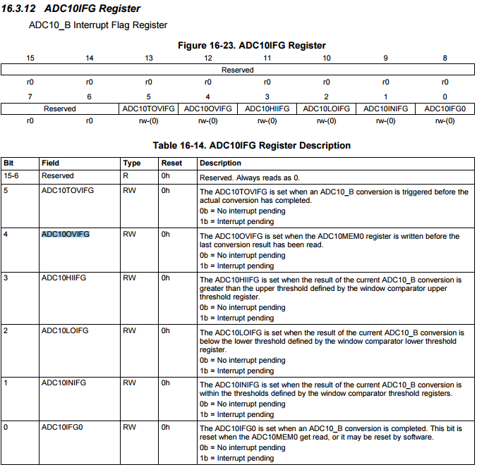
  • Also, looking at Cycle 2, the ADC10IFG Interrupt Flag is equal to 0x0012. According to Section 16.3.12 in the User's Guide, this means that the ADC10OVIFG and ADC10INIFG flags are set.

    ADC10OVIFG gets set when the ADC10MEM0 register is written before the last conversion result has been read.

    Regards,

    James

    MSP Customer Applications

**Attention** This is a public forum