This thread has been locked.

If you have a related question, please click the "Ask a related question" button in the top right corner. The newly created question will be automatically linked to this question.

MSP430G2553: Regarding INFO Segment Erase

Part Number: MSP430G2553
Other Parts Discussed in Thread: MSP-FLASHER, UNIFLASH

Hi team,

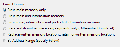
Here is screen shot of memory dump of one of the device in which all the segments of INFO locations are erased.


You can ignore those few locations at (0x103c)that are updated after the erase during subsequent power-up.


Here are few items: 

  1. Is it possible to erase INFOA segment without toggling LOCKA bit in FCTL3 (any errata). There are NO lines in CODE to toggle this bit. Not sure of its value on POR. Datasheet says as 1. How does writing a 1 to it clears this bit?
  2. Is it required to toggle LOCKA bit to erase all other INFO segments ??
  3. Is it required to Erase(segment/word) INFO FLASH before every write to it ??

  • Section 7.2.1 of the User's Guide says:

    SegmentA of the information memory is locked separately from all other segments with the LOCKA bit. When LOCKA = 1, SegmentA cannot be written or erased and all information memory is protected from erasure during a mass erase or production programming. When LOCKA = 0, SegmentA can be erased and written as any other flash memory segment, and all information memory is erased during a mass erase or production programming.

    The state of the LOCKA bit is toggled when a 1 is written to it. Writing a 0 to LOCKA has no effect. This allows existing flash programming routines to be used unchanged.

    Like any other flash memory, erasing sets all bits to 1, and programming sets some bits to 0.

  • Hi PengYu,

    It sounds like you are seeing all of INFO memory, not just INFOA, being erased unexpectedly - is that correct?

    1. It should not be possible to erase INFOA without toggling the LOCKA bit to be cleared in FCTL3 by writing a 1 to it (and I'm not aware of any errata that do this). LOCKA in the user's guide states that it should come up as 1 at a PUC. The LOCKA is toggled by writing a 1 to it. The other way that the LOCKA bit can be cleared would be by the toolchain - if you have selected in CCS, IAR, MSP-FLASHER, MSP-GANG etc that you want INFO and protected INFOA to be cleared at programming time, then the tool chain is going to clear LOCKA so that the mass erase can erase all info memory.

    2. It is required to clear LOCKA in order to erase other INFO segments with a MASS erase. You can still do segment erases to clear the other INFO segments without having to clear LOCKA, but the other INFO segments won't be cleared on a MASS erase if LOCKA is set.

    3. It is not required to erase INFO flash before every write necessarily - it depends on what you are doing. Like all FLASH, bits can only be set to 1 by an erase and only set to 0 by a write. So if you want to write an address that has previously been written to, and could have some bits needing to be 1 that weren't 1 before, you definitely have to do an erase. You also don't want to write to the same line of flash over and over without an erase because you can end up violating the cumulative programming time in the datasheet. Please see MSP430 Flash Memory Characteristics app note www.ti.com/lit/pdf/slaa334 for more information about flash handling and interpreting the cumulative programming time in the datasheet. Basically erasing periodically if you are doing many many writes is needed to refresh the cells.

    For your present situation, are you seeing this issue of INFOA being erased immediately after first programming? If so, how are you programming the part (what tool like CCS or IAR IDE, MSP-FLASHER, MSP-GANG, Uniflash, FET-PRO430 etc)? In CCS for example, there are separate options to erase information memory while still keeping protected information memory (INFOA), vs other options to erase both.

    Regards,

    Katie

**Attention** This is a public forum