Because of the holidays, TI E2E™ design support forum responses will be delayed from Dec. 25 through Jan. 2. Thank you for your patience.

This thread has been locked.

If you have a related question, please click the "Ask a related question" button in the top right corner. The newly created question will be automatically linked to this question.

MSP430G2553: multiple msp430 programming using master MCU (msp430)

Part Number: MSP430G2553
Other Parts Discussed in Thread: MSP430F5659, MSP430FR6989, MSP-GANG,

hi

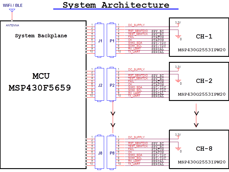
in our project We will have one backplane contains MSP430F5659 MCU that should communicate and program 8 channels containing  MSP430G2553IPW20 MCU’s,

This backplane will have TI’s selected WiFi/BLE solution & USB as well.

In order to proper design the hardware infrastructure, we must know if there is a simple way using the BSL to run and program each one of the 8 channels in sequence.

That will be uses for future firmware upgrades via WiFi and/or BLE and/or USB (upon user needs).

Looking at attached scheme my infrastructure able to use I2C , TX/RX (uart) and SBW as well.

 we would like to know:

  1. What is the best recommended method to do it ? (I2C , TX/RX or SBW ?).
  2. Do you have any sample code ?
  3. Any additional information/recommendation ?


  • 2553 is with UART ROM BSL, that can not be changed. So if you want to go by BSL, UART must be used with TEST / RESET pins for BSL entry sequence, and TX / RX for data exchange. Master side as open source (slau319) can be found here...

    http://www.ti.com/tool/mspbsl

    SBW use only 2 pins (TEST / RESET) for entry sequence and data exchange. And from my point of view, it is better choice for target device firmware update than BSL. TI debug stack (FET firmware for SBW / JTAG) is open source...

    http://www.ti.com/tool/MSPDS

    There is also slau320 / Replicator, that is open source...

    http://www.ti.com/tool/REP430F

  • hi

    many thanks for your quick reply

    however regarding the scheme we sent , can you suggest how to use SBW and or TEST / RESET controls to program multiple MSP430`s from a master MSP430 (not from a PC) ?

    Do you have any Sample code that showing that ?

    thanks.

    avi
  • Avi Cohen said:


    however regarding the scheme we sent , can you suggest how to use SBW and or TEST / RESET controls to program multiple MSP430`s from a master MSP430 (not from a PC) ?

    Do you have any Sample code that showing that ?

    As I already mention, you can find this on Replicator page...

    http://www.ti.com/lit/pdf/slau320

    http://www.ti.com/lit/zip/slau320

    If you don't need SBW / JTAG fuse blow option (and I guess that you don't need it), than two port pins from master device are directly connected to TEST / RESET pin of target device. In total, 16 pins from master device to 8 TEST and 8 RESET pins on target device. Of course, master and target device(s) should be on the same VCC / GND lines.

    Same thing you can see in open source (software / hardware) TI eZ-FET Lite that is included in TI launchpads.

  • hi,

    is there any similar code as that replicator project for host msp430fr6989 ?  or similar to MSp430FRxxx series?

    thanks.

    avi

  • No, but this (master) is irrelevant here, because for SBW / JTAG standard I/O port switching for SBW / JTAG shiftings is used, and there is no need for any (master) family device specific hardware module / peripheral. You just need to take from replicator code parts that you need (related to target flash 2xx family), and adopt it to your master device (I/O). If for you is enough that master program all target devices sequentially one by one, and not in parallel at once, than extracting number of targets from 1 (replicator code) to 8 is easy.

  • Hi

    Thanks once again for your support

    However it is still unclear.  You always mention that if we are using sbw 2 wires  we can use  standards IO.  It might be right for one device and not for 8. We bassically need 5 wires from the host controllers to be connected to 2 wires in the target device.

    1 io will be connected to the Target Test pin  and the 4 rest Wires needs to be connected in serial to Target Reset pin.

    I also do not understand why the host is irrelevant.  We need to store the target firmware.  In our application no PC is connected.  It should be 100% stand alone device.

    Thanks

  • I guess that master and target device already share VCC / GND lines. For SBW you just need 2 more lines, any (free) IO port pin on master side and TEST / RESET on target device side.  For example, it should be like this...

    master      CH1

       VCC ---> VCC

       GND ---> GND

      P1.0 ---> RESET

      P2.0 ---> TEST

                 CH2

        VCC ---> VCC

       GND ---> GND

      P1.1 ---> RESET

      P2.1 ---> TEST

    .....

                CH8

       VCC ---> VCC

       GND ---> GND

      P1.7 ---> RESET

      P2.7 ---> TEST


    2 ports / 16 pins should be used on master side for complete SBW connection.

    Master device is irrelevant because (at the end) you code regarding SBW flashing will be portable between any 5xx device.

  • Hi.

    Thanks again

    Did you had ever that kind of project or it is only theory?

    Again. It is unclear.  Each gpio had its own features.  Dont we need a gpio that has clk  or sny special requirement from the IO  ?

    I appriciate your kind support but we have read a lot of info and it doesnt fit your suggestion.

    Thanks.

  • I am the author of SBW+ flasher. It is MSP-GANG like device (8 targets) using SBW extended by one more IO line for increasing transfer rate (SBW bottleneck) between master and target devices (up to 200 KByte / sec). I started from slau320, because at that time MSP Debug Stack was not open source.

    Port pin (bit) should be used for writing 0 / 1 and reading. TEST is only master output (target device input), RESET is (changing direction) input / output. Peripherals (gpio features, clk / some special requirement) are not needed (and AFAIK they are not used in slau320).

  • Once again. Thanks for the support

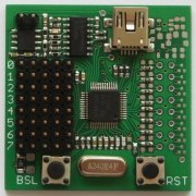
    Can you share info of the image you showing here?  Thats look what we are want to applied in our project.

    We saw many projects that use pc side.  Our project must be stand alone device,  that in future we will get the firmware by wifi or BLE,  we allready testing cc3220 devices.

    There is not standalone projects examples for 2 wire sbw.  (replicator has all jtag options)

    Thanks.

  • SBW+ flasher is working with PC side, and USB as hart. It was developed with speed as main task, coded from zero, completely in assembler, with slau320 as reference. There is no buffer limitation, complete file from PC is sent over USB at once. Data transfer PC / SBW+ Flasher /  Target devices is going in parallel, without any latency.

    Flashing 2xx

    Flashing 5xx

    Flashing sequentially different family with different firmware

    Integrated in Energia

    Benchmark

    This is completely different animal from updating target devices with firmware received over wifi / BLE, where speed is not so important, and firmware size is irrelevant (much smaller than 512 KByte). It is much easier to flash target devices with prepared firmware, stored in master device RAM / FRAM / Flash. My Flasher use peripherals, and port with mapping option is reserved for RESET lines. It also request one extra line (PIO) between master and target device. You can contact me by PM to see if part of my work can be rebuild and used in your project.

    Anyway, receiving and preparing firmware for flashing is up to you (but If I remember right, there are TI open source examples for this), and all regarding MSP430G2553 SBW flashing can be imported from replicator code (#ifdef SPYBIWIRE_MODE). You don't need replicator hardware. Simply extend replicator flashing (in source code) of one target device to sequentially eight, one by one.

**Attention** This is a public forum