This thread has been locked.

If you have a related question, please click the "Ask a related question" button in the top right corner. The newly created question will be automatically linked to this question.

MSP430G2955: timer problem does not count external clocks from certain pin oscillator

Part Number: MSP430G2955

hello Everyone,

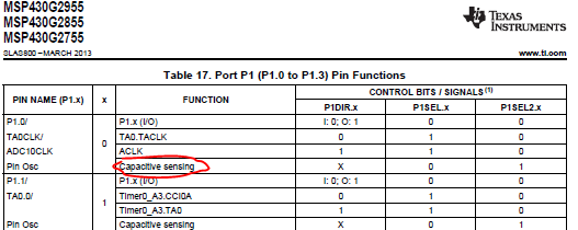
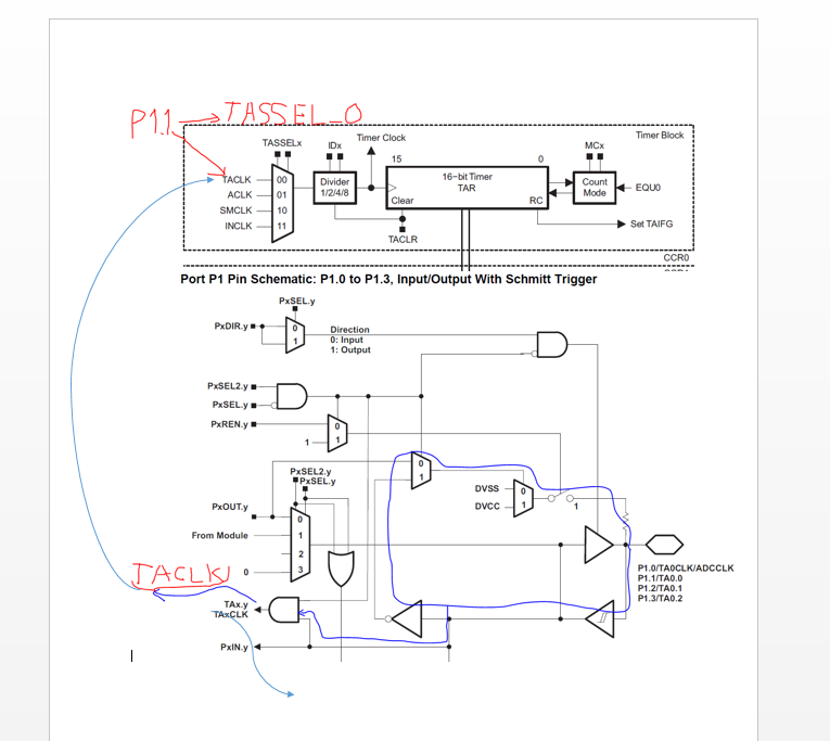
before i explain my issue, i have some difficulties to unerstand the difference between the TA0CLK,TA0.0, TA0.1 and TA0.2 and their functionalities.according to what i know there are only 3 timers in my MSP430G2955 timer0.A3, timer1.A3 and timer0.B3 so i don't find any relation between them

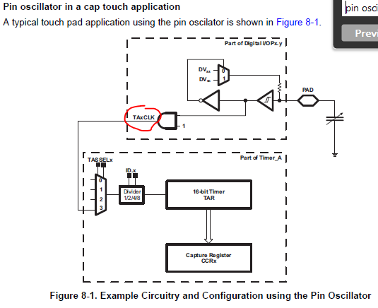
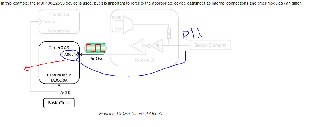
my conern why only the P1.0 is counting the external clock(PIN Oscillator) ,is it becaue it has TA0CLK or something i don't know? please halp me out because none of the documantation say anything about it.below you find the pictures of what it is given by the data sheet

  • Hello tarik,

    Timer functions are captured in Table 2 of the datasheet.

    TA0CLK: Optional input clock source for TA0, selectable through the TASSELx bits of the TACTL register.
    TA0.0-TA0.2: CCI0A-CCI2A inputs in capture mode, CCR0-CCR2 outputs in compare mode.

    All of these pins mentioned refer to TA0_A3, further explained in Table 12. Capacitive sensing mode is a different function from TA0 (as shown through the P1SEL/P1SEL2 register bit settings shown in Table 17). For the Capacitive Touch Software Library, TA0 is driven internally by an on-board clock source and does not require TA0CLK input which frees P1.0 for Pin Osc functionality.

    As the CAPSENSELIBRARY is a legacy product I would recommend that you look into CapTIvate technology for new product design, the MSP-CAPT-FR2633 page would be a great starting point.

    Regards,
    Ryan
  • Hello Ryan,

    thank you for your answer,

    -i am still having trouble to undesrand what is TA0.0 TA0.1 and TA0.2 i mean what are they? i understood from your comment that they are pins but i don't find them in the Figure 12-1. Timer_A Block Diagram of slau144j.pdf, i understand that the 3 refers to 03 capture/compare channel that the timer has.

    -according to what you said (TA0CLK: Optional input clock source for TA0, selectable through the TASSELx bits of the TACTL register.) how can i connect the pin P1.1 to timer0_A3 using the TASSELx bits of the TACTL register? ihave done it for pin P1.0 and works perfecly as you can sse in the code below but have no idea for P1.1, because in Table 12. Timer0_A3 Signal Connections i see that there are difference between them .

    -thank you for the link of the library, i am on it now but i want to understand the routing of signla for the pins so i understand ver well the library without using it blindly and not understanding how the registers are set an their roles.

    TA0CTL =TASSEL_0|ID_3|MC_2|TACLR;               
    TA0CCTL0 =CM_3|CCIS_2|CAP;
  • sorry, i meant in the second paragragh, how i can make the oin P1.1 as external clock for the timer0_A3?
  • Hi tarik,

    You see TA0.0-TA0.2 as CCR0-CCR2 in Figure 12-1, only CCR2 is shown to limit redundancy. Switching between capture (output) and compare (input) modes are selected by the CAP bit of the TACCTLx register.

    The code shown is for P1.1/TA0.0 so long as you set TACCR0 for the correct period. Now all that is required is the proper P1SEL bit assignments. P1.0/TACLK is for a TACLK input if desired.

    You really should refer to the timer examples provided by TI to get a better grasp on how to control these modules properly.

    Regards,
    Ryan
  •  Hello Ryan,

    thank you of the advice for the timer,it was helpfull. so to make sure that i am not in understand it. it is not only the pin P1.0 which can be assigned as clock input for the timer0_A3 (TAR). so what are they doing in the capacitive touch library is first set the timer input clock to external as shown below:

    TA0CTL =TASSEL_0|ID_3|MC_2|TACLR;

    secondly setting the P1SEL and P2SEL like following:

    P1DIR &= ~ BIT1;                    //P1.1

    P1SEL &= ~ BIT1;

    P1SEL2 |= BIT1;                            // activating the pin oscillation

    this should feed the timer0_A3 by the pin oscillation

    here i have a pic of what i understood

  • Please state the Cap Touch example project you are referencing. You will see from Section 3 of SLAA363 that such an external connection setup typically required a comparator output into TACLK, when your G2xxx5 device should solely be using the Pin Oscillator peripheral. I also recommend SLAA490/491 for a better understanding of the CAPSENSELIBRARY.

    Regards,
    Ryan
  •   Yes as you can see in the picture, i did it for P1.0 without using the comparator, my method for P1.0 works perfectly nice without using the comparaor because i use the ethod given in this link:

    http://processors.wiki.ti.com/index.php/MSP430_Low_Cost_PinOsc_Capacitive_Touch_Overview

  • Glad to hear it, sounds like you are on top of things then.

    Regards,
    Ryan
  • i understand the concept for this situation however i have no clue why the Pin P1.1 does need feed the timer with clock? why only pin P1.0 works(timer0_A3 counting the clocks coming from the Pin P1.0 only)?
  • P1.1 is required to drive the sensor with a PinOsc waveform. Only P1.0 works since a TACLK input in needed. Please further read the CAPSENSELIBRARY documentation in detail to get a better understanding of this technology.

    Regards,
    Ryan

**Attention** This is a public forum