This thread has been locked.

If you have a related question, please click the "Ask a related question" button in the top right corner. The newly created question will be automatically linked to this question.

MSP432P401R: Sampling Audio and Storing with DMA

Part Number: MSP432P401R

My end goal for this project is to sample audio from an amplified electret microphone, and store it in SRAM (short sample, I know) using DMA. 

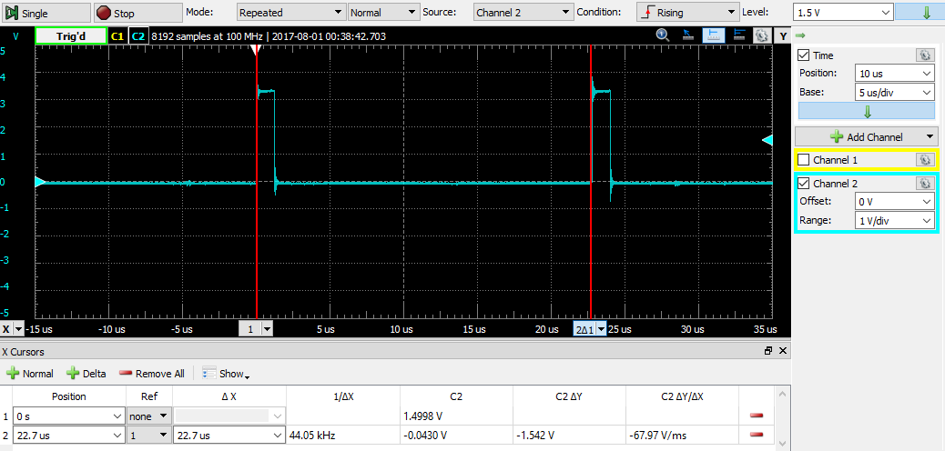
Currently, the output of my microphone circuit looks perfect through an oscilloscope. I'm running my MSP432 at 48 MHz; so I should be able to sample at 44.1 kHz without a problem, though I will probably sample slower just to save RAM. 

My ideal scenario is as follows: 

  1. Automatically trigger ADC conversions at a rate of 44.1 kHz using Timer_A0. 
  2. When each conversion is completed, automatically transfer sample to memory.

The problem I am running into is that I can't get the ADC to trigger automatically using a timer. I can't find any example code that doesn't use the DriverLib API. 

So FOR NOW, I am trying to manually trigger a conversion at 44.1 kHz using a timer interrupt. I configured Timer_A0 in UP mode, with a CCR0 value that triggers a timer overflow interrupt at a rate of 44.1 kHz. So my timer is working perfectly, but when I start a conversion inside my timer interrupt function (and manually store the data inside a conversion complete interrupt), I get wonky ADC results when I look at the data after pausing the program. 

Here is my code as of now: 

#include "msp.h"

#define A0 BIT5

#define num_samples 100

#define startConversion() ADC14->CTL0 |= ADC14_CTL0_ENC | ADC14_CTL0_SC

#define startSampling() TIMER_A0->CCR[0] =	271 // Corresponds to 44.1 kHz sampling rate
#define stopSampling() TIMER_A0->CCR[0] = 0;

void VCORE1();
void FLASH_init();
void CLK_init();
void ADC_init();
void TIMER_init();

volatile uint16_t audio[num_samples];
volatile uint16_t i = 0;

void main(void)
{
	WDT_A->CTL = WDT_A_CTL_PW | WDT_A_CTL_HOLD;		// stop watchdog timer

	//P2->DIR |= BIT7;

	//Enable MCLK clock output on P4.3
	//P4->DIR |= BIT3;
	//P4->SEL0 |= BIT3;

	VCORE1();				//Go to VCORE1 mode before setting clock to 48 MHz
	FLASH_init();
	CLK_init();				//Set clock to 48 MHz
	ADC_init();				//Initializes ADC, waiting for Timer to start conversions
	TIMER_init();

	NVIC_EnableIRQ(ADC14_IRQn);
	NVIC_EnableIRQ(TA0_0_IRQn);

	__enable_irq();

	startSampling();

	while(1);
}

void ADC14_IRQHandler(void)
{
	audio[i] = ADC14->MEM[0];	//Save sample, clears flag
}

void TA0_0_IRQHandler(void)
{
	TIMER_A0->CCTL[0] &= ~TIMER_A_CCTLN_CCIFG;	//Clear timer flag
	//P2->OUT |= BIT7; //For testing timer
	startConversion();
}

void VCORE1()
{
	while(PCM->CTL1 & PCM_CTL1_PMR_BUSY);
	PCM->CTL0 = PCM_CTL0_KEY_VAL | PCM_CTL0_AMR__AM_LDO_VCORE1;
	while(PCM->CTL1 & PCM_CTL1_PMR_BUSY);
}

void FLASH_init()
{
	//Configure Flash wait-state to 1 for both banks 0 & 1
	FLCTL->BANK0_RDCTL = (FLCTL->BANK0_RDCTL & ~(FLCTL_BANK0_RDCTL_WAIT_MASK)) |
			FLCTL_BANK0_RDCTL_WAIT_1;
	FLCTL->BANK1_RDCTL  = (FLCTL->BANK0_RDCTL & ~(FLCTL_BANK1_RDCTL_WAIT_MASK)) |
			FLCTL_BANK1_RDCTL_WAIT_1;
}

void CLK_init()
{
	//Set clock to 48 MHz
	CS->KEY 	= 	CS_KEY_VAL;				//Unlock CS registers
	CS->CTL0 	= 	CS_CTL0_DCOEN 	|
					CS_CTL0_DCORSEL_5;		//Choose 24MHz MHz clock speed
	CS->CTL1 	= 	CS_CTL1_SELS_3 	|
					CS_CTL1_SELM_3;			//Use DCOCLK as source for MCLK, SMCLK + HSMCLK
	CS->KEY		=	0;						//Re-lock CS registers
}

void ADC_init()
{
	P5->DIR &= ~(A0);	//Set ADC pin as input

	P5->SEL0 |= A0;		//Choose ADC as port function
	P5->SEL1 |= A0;

	ADC14->CTL0	=	//ADC14_CTL0_SHS_1	|	//Use TA0 to start conversion
					ADC14_CTL0_SHP	 	|	//??
					ADC14_CTL0_ON;		 	//Turn ADC module on
	ADC14->CTL1	=	ADC14_CTL1_RES__14BIT;	//Set 14-bit resolution
	ADC14->IER0 = 	ADC14_IER0_IE0;			//Enable interrupt when conversion on A0 is complete
}

void TIMER_init()
{
	TIMER_A0->CCTL[0] 	=	TIMER_A_CCTLN_CCIE;			//Enable CC interrupt

	TIMER_A0->CTL 		=	TIMER_A_CTL_TASSEL_2 	|	//Select SMCLK as source for timer
							TIMER_A_CTL_ID_2		|	//Divide clock by 4 (this yields 6 MHz for the timer clock)
							TIMER_A_CTL_MC_1		|	//Up mode
							TIMER_A_CTL_CLR			;	//Clear timer count

}

  • Wes,

       The timer trigger definition is found in the ADC14CTL0 register and in the datasheet.   So for example if you wanted to trigger the timer from TA0.1 you would pick ADC14SHSx = 1.

    I would recommend using the driverLib examples.  I found one here:

    Also, here is another attached:

    /*
     * -------------------------------------------
     *    MSP432 DriverLib - v3_10_00_09 
     * -------------------------------------------
     *
     * --COPYRIGHT--,BSD,BSD
     * Copyright (c) 2014, Texas Instruments Incorporated
     * All rights reserved.
     *
     * Redistribution and use in source and binary forms, with or without
     * modification, are permitted provided that the following conditions
     * are met:
     *
     * *  Redistributions of source code must retain the above copyright
     *    notice, this list of conditions and the following disclaimer.
     *
     * *  Redistributions in binary form must reproduce the above copyright
     *    notice, this list of conditions and the following disclaimer in the
     *    documentation and/or other materials provided with the distribution.
     *
     * *  Neither the name of Texas Instruments Incorporated nor the names of
     *    its contributors may be used to endorse or promote products derived
     *    from this software without specific prior written permission.
     *
     * THIS SOFTWARE IS PROVIDED BY THE COPYRIGHT HOLDERS AND CONTRIBUTORS "AS IS"
     * AND ANY EXPRESS OR IMPLIED WARRANTIES, INCLUDING, BUT NOT LIMITED TO,
     * THE IMPLIED WARRANTIES OF MERCHANTABILITY AND FITNESS FOR A PARTICULAR
     * PURPOSE ARE DISCLAIMED. IN NO EVENT SHALL THE COPYRIGHT OWNER OR
     * CONTRIBUTORS BE LIABLE FOR ANY DIRECT, INDIRECT, INCIDENTAL, SPECIAL,
     * EXEMPLARY, OR CONSEQUENTIAL DAMAGES (INCLUDING, BUT NOT LIMITED TO,
     * PROCUREMENT OF SUBSTITUTE GOODS OR SERVICES; LOSS OF USE, DATA, OR PROFITS;
     * OR BUSINESS INTERRUPTION) HOWEVER CAUSED AND ON ANY THEORY OF LIABILITY,
     * WHETHER IN CONTRACT, STRICT LIABILITY, OR TORT (INCLUDING NEGLIGENCE OR
     * OTHERWISE) ARISING IN ANY WAY OUT OF THE USE OF THIS SOFTWARE,
     * EVEN IF ADVISED OF THE POSSIBILITY OF SUCH DAMAGE.
     * --/COPYRIGHT--*/
    /*******************************************************************************
     * MSP432 ADC14 - Single Channel Repeated Sample w/ Timer_A Trigger
     *
     * Description: In this ADC14 code example, a single input channel is sampled
     * using the standard 3.3v reference. The source of the sample trigger for this
     * example is Timer_A CCR1. The ADC is setup to repeatedly sample/convert
     * from A0 when triggered from TIMERA0.  The DMA is used in ping-pong mode and
     * triggered by the dma to store the conversion results.
     *
     * The PWM is started once the GPIO interrupt for P1.1 is serviced.
     *
     *                MSP432P401
     *             ------------------
     *         /|\|                  |
     *          | |                  |
     *          --|RST         P4.7  |<--- A6, Ain+
     *            |            P4.6  |<--- A7, Ain-
     *            |                  |
     *            |            P1.1  |<--- GPIO trigger to Start conversions
     *            |                  |
     *            |            P1.0  |---> Debug port to show ADC ISR
     *            |            P2.4  |---> Debug TA0.1, ADC trigger
     *            |                  |
     *
     * Author: T. Logan/ C. Sterzik
     ******************************************************************************/
    /* DriverLib Includes */
    #include <ti/devices/msp432p4xx/driverlib/driverlib.h>
    
    /* Standard Includes */
    #include <stdint.h>
    #include <stdbool.h>
    
    #define ARRAY_LENGTH    256
    
    /*
     * Timer_A Compare Configuration Parameter
     * CCR1 is used to trigger the ADC14, conversion time
     * SMCLK = 24Mhz, Timer = 10Khz
     */
    const Timer_A_PWMConfig timerA_PWM =
    {
        .clockSource = TIMER_A_CLOCKSOURCE_SMCLK,
        .clockSourceDivider = TIMER_A_CLOCKSOURCE_DIVIDER_1,
        .timerPeriod = 2399,
        .compareRegister = TIMER_A_CAPTURECOMPARE_REGISTER_1,
        .compareOutputMode TIMER_A_OUTPUTMODE_SET_RESET,
        .dutyCycle = 1200
    };
    
    /* DMA Control Table */
    #if defined(__TI_COMPILER_VERSION__)
    #pragma DATA_ALIGN(MSP_EXP432P401RLP_DMAControlTable, 1024)
    #elif defined(__IAR_SYSTEMS_ICC__)
    #pragma data_alignment=1024
    #elif defined(__GNUC__)
    __attribute__ ((aligned (1024)))
    #elif defined(__CC_ARM)
    __align(1024)
    #endif
    static DMA_ControlTable MSP_EXP432P401RLP_DMAControlTable[16];
    
    /* Statics */
    static volatile uint16_t resultsBufferPrimary[ARRAY_LENGTH];
    static volatile uint16_t resultsBufferAlternate[ARRAY_LENGTH];
    
    int main(void)
    {
        /* Halting WDT  */
        MAP_WDT_A_holdTimer();
        MAP_Interrupt_enableSleepOnIsrExit();
    
        /*
         * Starting HFXT in non-bypass mode without a timeout. Before we start
         * we have to change VCORE to 1 to support the 48MHz frequency
         */
        MAP_PCM_setCoreVoltageLevel(PCM_VCORE1);
    
        /*
         * Revision C silicon supports wait states of 1 at 48Mhz
         */
        MAP_FlashCtl_setWaitState(FLASH_BANK0, 1);
        MAP_FlashCtl_setWaitState(FLASH_BANK1, 1);
    
        /*
         * Setting up clocks
         * MCLK = MCLK = 48MHz
         * SMCLK = MCLK/2 = 24Mhz
         * ACLK = REFO = 32Khz
         */
        MAP_CS_setDCOFrequency(48000000);
        MAP_CS_initClockSignal(CS_ACLK, CS_REFOCLK_SELECT, CS_CLOCK_DIVIDER_1);
        MAP_CS_initClockSignal(CS_SMCLK, CS_DCOCLK_SELECT, CS_CLOCK_DIVIDER_2);
        MAP_CS_initClockSignal(CS_MCLK, CS_DCOCLK_SELECT, CS_CLOCK_DIVIDER_1);
    
        /* Initializing ADC (SMCLK/1/1) */
        MAP_ADC14_enableModule();
        MAP_ADC14_initModule(ADC_CLOCKSOURCE_SMCLK, ADC_PREDIVIDER_1, ADC_DIVIDER_1,
                0);
    
        /*
         * Debug
         * Configuring P1.0 as output
         */
        MAP_GPIO_setAsOutputPin(GPIO_PORT_P1, GPIO_PIN0);
        P1OUT &= ~BIT0;
    
        /*
         * Configuring GPIOs (4.6 A7, 4.7 A6)
         */
        MAP_GPIO_setAsPeripheralModuleFunctionInputPin(GPIO_PORT_P6, (GPIO_PIN6+GPIO_PIN7),
        GPIO_TERTIARY_MODULE_FUNCTION);
    
        /*
         * Debug: set TA0.1 as output to see ADC trigger signal
         */
        MAP_GPIO_setAsPeripheralModuleFunctionOutputPin(GPIO_PORT_P2, GPIO_PIN4,
        GPIO_PRIMARY_MODULE_FUNCTION);
    
        /*
         * Configuring P1.1 as an input and enabling interrupt, the timer is started from
         * GPIO ISR.
         */
        MAP_GPIO_setAsInputPinWithPullUpResistor(GPIO_PORT_P1, GPIO_PIN1);
        MAP_GPIO_interruptEdgeSelect(GPIO_PORT_P1,GPIO_PIN1,GPIO_HIGH_TO_LOW_TRANSITION);
        MAP_GPIO_clearInterruptFlag(GPIO_PORT_P1, GPIO_PIN1);
        MAP_GPIO_enableInterrupt(GPIO_PORT_P1, GPIO_PIN1);
    
        MAP_REF_A_setReferenceVoltage(REF_A_VREF2_5V);
        MAP_REF_A_enableReferenceVoltage();
    
        /*
         * Configuring ADC Memory, repeat-single-channel, A0
         */
        MAP_ADC14_configureSingleSampleMode(ADC_MEM0, true);
        /*
         * Configuring ADC Memory, reference, and differential conversion
         * A0 goes to mem0, AVcc is the reference, and the conversion is
         * single-ended
         */
        MAP_ADC14_configureConversionMemory(ADC_MEM0, ADC_VREFPOS_INTBUF_VREFNEG_VSS,
        ADC_INPUT_A6, ADC_DIFFERENTIAL_INPUTS);
        /*
         * Configuring the sample trigger to be sourced from Timer_A0 CCR1 and on the
         * rising edge, default samplemode is extended (SHP=0)
         */
        MAP_ADC14_setSampleHoldTrigger(ADC_TRIGGER_SOURCE1, false);
        MAP_ADC14_setSampleHoldTime(ADC_PULSE_WIDTH_8,ADC_PULSE_WIDTH_8);
    
        /*
         * Enabling  conversions
         */
        MAP_ADC14_enableConversion();
    
        /* Configuring DMA module */
        MAP_DMA_enableModule();
        MAP_DMA_setControlBase(MSP_EXP432P401RLP_DMAControlTable);
    
        /*
         * Setup the DMA + ADC14 interface
         */
        MAP_DMA_disableChannelAttribute(DMA_CH7_ADC14,
                                     UDMA_ATTR_ALTSELECT | UDMA_ATTR_USEBURST |
                                     UDMA_ATTR_HIGH_PRIORITY |
                                     UDMA_ATTR_REQMASK);
    
        /*
         * Setting Control Indexes. In this case we will set the source of the
         * DMA transfer to ADC14 Memory 0 and the destination to the destination
         * data array.
         */
        MAP_DMA_setChannelControl(UDMA_PRI_SELECT | DMA_CH7_ADC14,
                UDMA_SIZE_16 | UDMA_SRC_INC_NONE | UDMA_DST_INC_16 | UDMA_ARB_1);
        MAP_DMA_setChannelTransfer(UDMA_PRI_SELECT | DMA_CH7_ADC14,
                UDMA_MODE_PINGPONG, (void*) &ADC14->MEM[0],
                (void*)resultsBufferPrimary, ARRAY_LENGTH);
        MAP_DMA_setChannelControl(UDMA_ALT_SELECT | DMA_CH7_ADC14,
                UDMA_SIZE_16 | UDMA_SRC_INC_NONE | UDMA_DST_INC_16 | UDMA_ARB_1);
        MAP_DMA_setChannelTransfer(UDMA_ALT_SELECT | DMA_CH7_ADC14,
                UDMA_MODE_PINGPONG, (void*) &ADC14->MEM[0],
                (void*)resultsBufferAlternate, ARRAY_LENGTH);
    
        /* Assigning/Enabling Interrupts */
        MAP_DMA_assignInterrupt(DMA_INT1, 7);
        MAP_DMA_assignChannel(DMA_CH7_ADC14);
        MAP_DMA_clearInterruptFlag(7);
    
        /* Enabling Interrupts */
        MAP_Interrupt_enableInterrupt(INT_DMA_INT1);
        MAP_Interrupt_enableInterrupt(INT_PORT1);
        MAP_Interrupt_enableMaster();
    
        /* Going to sleep */
        MAP_PCM_gotoLPM0();
        __no_operation();
    }
    
    /* Completion interrupt for ADC14 MEM0 */
    __attribute__((ramfunc))  // Requires compiler TI v15.12.1.LTS
    void DMA_INT1_IRQHandler(void)
    {
        P1->OUT |= BIT0;
        /*
         * Switch between primary and alternate bufferes with DMA's PingPong mode
         */
        if (MAP_DMA_getChannelAttribute(7) & UDMA_ATTR_ALTSELECT)
        {
    //        MAP_DMA_setChannelControl(UDMA_PRI_SELECT | DMA_CH7_ADC14,
    //              UDMA_SIZE_16 | UDMA_SRC_INC_NONE | UDMA_DST_INC_16 | UDMA_ARB_1);
    //        MAP_DMA_setChannelTransfer(UDMA_PRI_SELECT | DMA_CH7_ADC14,
    //              UDMA_MODE_PINGPONG, (void*) &ADC14->MEM[0],
    //              resultsBufferPrimary, ARRAY_LENGTH);
            MSP_EXP432P401RLP_DMAControlTable[7].control =
                    (MSP_EXP432P401RLP_DMAControlTable[7].control & 0xff000000 ) |
                    (((ARRAY_LENGTH)-1)<<4) | 0x03;
        }
        else
        {
    //        MAP_DMA_setChannelControl(UDMA_ALT_SELECT | DMA_CH7_ADC14,
    //              UDMA_SIZE_16 | UDMA_SRC_INC_NONE | UDMA_DST_INC_16 | UDMA_ARB_1);
    //        MAP_DMA_setChannelTransfer(UDMA_ALT_SELECT | DMA_CH7_ADC14,
    //              UDMA_MODE_PINGPONG, (void*) &ADC14->MEM[0],
    //              resultsBufferAlternate, ARRAY_LENGTH);
            MAP_Timer_A_stopTimer(TIMER_A0_BASE);
            MAP_DMA_disableChannel(7);
            /*
             * ISR is being called twice at the end.  Need to investigate further.
             */
            MAP_DMA_clearInterruptFlag(7);
            MSP_EXP432P401RLP_DMAControlTable[15].control =
                    (MSP_EXP432P401RLP_DMAControlTable[15].control & 0xff000000 ) |
                    (((ARRAY_LENGTH)-1)<<4) | 0x03;
        }
        P1->OUT &= ~BIT0;
    }
    
    void PORT1_IRQHandler(void)
    {
        P1->OUT |= BIT0;
        P1IFG &= ~BIT1;
        MAP_DMA_enableChannel(7);
        MAP_Timer_A_generatePWM(TIMER_A0_BASE, &timerA_PWM);
        P1->OUT &= ~BIT0;
    }
    

    In both cases the DMA 'ping-pong' is used so that you can process one set of data while capturing the next.

    Regards,
    Chris

  • Is your signal ground referenced or DC-offset? The MSP432 does not like negative voltage inputs.
  • Chris Sterzik said:
    So for example if you wanted to trigger the timer from TA0.1 you would pick ADC14SHSx = 1.

    After doing some more research, I figured a lot out. I was assuming it would automatically start a conversion when the timer overflowed. 

    I now have CCR0 set to the same value to yield samples at 44.1 kHz, AND I have a CCR1 value that will act as a way to initiate the ADC. See the screenshot below. 

    For this to work, I need to be in pulse sample mode, when ADC14SHP = 1. My timer just needs to output a rising edge pulse, which will trigger a sample and hold timer which I have configured to last 16 clock cycles (ADC14_CTL0_SHT0_2). I'm using ADC14MEM0, so I'm configuring the SHT0 bits. 

    Currently when I run my program, I get one ADC conversion, and then it never goes back into my ADC conversion complete interrupt function. 

    I will also include my current code below the screenshot. 

    #include "msp.h"
    
    #define A0 BIT5
    
    #define num_samples 1000
    
    #define startConversion() ADC14->CTL0 |= ADC14_CTL0_SC
    
    #define startSampling() TIMER_A0->CCR[0] =	271	// Corresponds to 44.1 kHz sampling rate
    #define stopSampling() TIMER_A0->CCR[0] = 0;
    
    void VCORE1();
    void FLASH_init();
    void CLK_init();
    void ADC_init();
    void TIMER_init();
    
    volatile uint16_t audio[num_samples];
    volatile uint16_t i = 0;
    
    void main(void)
    {
    	WDT_A->CTL = WDT_A_CTL_PW | WDT_A_CTL_HOLD;		// stop watchdog timer
    
    	P2->DIR |= BIT7;	//Debug output
    
    	P2->DIR |= BIT4;	//Debug TA0.1 output
    	P2->SEL0 |= BIT4;
    
    	VCORE1();				//Go to VCORE1 mode before setting clock to 48 MHz
    	FLASH_init();
    	CLK_init();				//Set clock to 48 MHz
    	ADC_init();				//Initializes ADC, waiting for Timer to start conversions
    	TIMER_init();
    
    	NVIC_EnableIRQ(ADC14_IRQn);
    
    	__enable_irq();
    
    	startSampling();
    
    	while(1);
    }
    
    void ADC14_IRQHandler(void)
    {
    	audio[0] = ADC14->MEM[0];	//Save sample, clears flag
    	P2->OUT ^= BIT7;			//Debug output
    }
    
    void VCORE1()
    {
    	while(PCM->CTL1 & PCM_CTL1_PMR_BUSY);
    	PCM->CTL0 = PCM_CTL0_KEY_VAL | PCM_CTL0_AMR__AM_LDO_VCORE1;
    	while(PCM->CTL1 & PCM_CTL1_PMR_BUSY);
    }
    
    void FLASH_init()
    {
    	//Configure Flash wait-state to 1 for both banks 0 & 1
    	FLCTL->BANK0_RDCTL = (FLCTL->BANK0_RDCTL & ~(FLCTL_BANK0_RDCTL_WAIT_MASK)) |
    			FLCTL_BANK0_RDCTL_WAIT_1;
    	FLCTL->BANK1_RDCTL  = (FLCTL->BANK0_RDCTL & ~(FLCTL_BANK1_RDCTL_WAIT_MASK)) |
    			FLCTL_BANK1_RDCTL_WAIT_1;
    }
    
    void CLK_init()
    {
    	//Set clock to 48 MHz
    	CS->KEY 	= 	CS_KEY_VAL;				//Unlock CS registers
    	CS->CTL0 	= 	CS_CTL0_DCOEN 	|
    					CS_CTL0_DCORSEL_5;		//Choose 48 MHz MHz clock speed
    
    	CS->CTL1 	= 	CS_CTL1_SELS_3 	|
    					CS_CTL1_SELM_3	;		//Use DCOCLK as source for MCLK, SMCLK + HSMCLK
    	CS->KEY		=	0;						//Re-lock CS registers
    }
    
    void ADC_init()
    {
    	P5->DIR &= ~(A0);	//Set ADC pin as input
    
    	P5->SEL0 |= A0;		//Choose ADC as port function
    	P5->SEL1 |= A0;
    
    	ADC14->CTL1	=	ADC14_CTL1_RES__14BIT;	//Set 14-bit resolution
    
    	ADC14->IER0 = 	ADC14_IER0_IE0;			//Enable interrupt when conversion on A0 is complete
    
    	ADC14->CTL0	=	ADC14_CTL0_SHS_1	|	//Use TA0 to start conversion
    					ADC14_CTL0_SHP	|		//Pulse mode
    					ADC14_CTL0_SHT0_2|		//16 clock cycles sample time
    					ADC14_CTL0_ON	|		//Turn ADC module ON
    					ADC14_CTL0_ENC	;		 //Enable conversions
    }
    
    void TIMER_init()
    {
    	TIMER_A0->CCTL[1] 	=	TIMER_A_CCTLN_OUTMOD_7;
    
    	TIMER_A0->CTL 		=	TIMER_A_CTL_TASSEL_2 	|	//Select SMCLK as source for timer
    							TIMER_A_CTL_ID_2		|	//Divide clock by 4 (this yields 12 MHz for the timer clock)
    							TIMER_A_CTL_MC_1		|	//Up mode
    							TIMER_A_CTL_CLR			;	//Clear timer count
    
    	TIMER_A0->CCR[1] = 100;
    }
    

  • Yes, the voltages I'm inputting are always between 0 and 3.3V (reference).
  • You need to select a repeat-single-channel mode:

    Regards,
    Chris

**Attention** This is a public forum