


Part Number: MSP430FR2533
Other Parts Discussed in Thread: MSP430FR2633
Hi MSP430 team
Customer use eUSCI_A1 and eUSCI_B0 SPI mode SIMO signal to drive RGB LED, related pin are P2.6, P1.2.
After using the same initial source code for eUSCI_A1 and eUSCI_B0, they found eUSCI_B0 P1.2 SIMO signal abnormal.
P2.6 can drive the RGB LEDs correctly, while P1.2 cannot drive LEDs correctly(first LED not work).
(两个SIMO信号分别驱动两串相同,做过交叉测试,确认原因是因为P1.2输出波形问题)。
From the capture waveform, it can find the P1.2 SIMO initial level is high, which may cause the issue.
Can you suggest why this happen?
Attached file is customer test P1.2 in TI MSPWARE example.
Initial code in customer project:
P2SEL0 |= (GPIO_PIN6); // set 3-SPI pin as second function
UCA1CTLW0 |= 0x0001; // **Put state machine in reset**
UCA1CTLW0 |= (0x01<<11)|(0x01<<8)|(0x01<<14)|(0x01<<13); // 3-pin, 8-bit SPI master
// Clock polarity high, MSB
UCA1CTLW0 |= (0x01<<7); // SMCLK
UCA1BR0 = 0x00; // /2,fBitClock = fBRCLK/(UCBRx+1).
UCA1BR1 = 0; //
UCA1MCTLW = 0; // No modulation
UCA1CTLW0 &= (0xfffe); // **Initialize USCI state machine**
P1SEL0 |= (GPIO_PIN2);
UCB0CTLW0 |= 0x0001;
UCB0CTLW0 |= (0x01<<11)|(0x01<<8)|(0x01<<14)|(0x01<<13); // 3-pin, 8-bit SPI master
// Clock polarity high, MSB
UCB0CTLW0 |= (0x01<<7); // SMCLK
UCB0BR0 = 0x00; // /2,fBitClock = fBRCLK/(UCBRx+1).
UCB0BR1 = 0; //
UCB0CTLW0 &= (0xfffe); // **Initialize USCI state machine**
/* --COPYRIGHT--,BSD
 * Copyright (c) 2016, Texas Instruments Incorporated
 * All rights reserved.
 *
 * Redistribution and use in source and binary forms, with or without
 * modification, are permitted provided that the following conditions
 * are met:
 *
 * *  Redistributions of source code must retain the above copyright
 *    notice, this list of conditions and the following disclaimer.
 *
 * *  Redistributions in binary form must reproduce the above copyright
 *    notice, this list of conditions and the following disclaimer in the
 *    documentation and/or other materials provided with the distribution.
 *
 * *  Neither the name of Texas Instruments Incorporated nor the names of
 *    its contributors may be used to endorse or promote products derived
 *    from this software without specific prior written permission.
 *
 * THIS SOFTWARE IS PROVIDED BY THE COPYRIGHT HOLDERS AND CONTRIBUTORS "AS IS"
 * AND ANY EXPRESS OR IMPLIED WARRANTIES, INCLUDING, BUT NOT LIMITED TO,
 * THE IMPLIED WARRANTIES OF MERCHANTABILITY AND FITNESS FOR A PARTICULAR
 * PURPOSE ARE DISCLAIMED. IN NO EVENT SHALL THE COPYRIGHT OWNER OR
 * CONTRIBUTORS BE LIABLE FOR ANY DIRECT, INDIRECT, INCIDENTAL, SPECIAL,
 * EXEMPLARY, OR CONSEQUENTIAL DAMAGES (INCLUDING, BUT NOT LIMITED TO,
 * PROCUREMENT OF SUBSTITUTE GOODS OR SERVICES; LOSS OF USE, DATA, OR PROFITS;
 * OR BUSINESS INTERRUPTION) HOWEVER CAUSED AND ON ANY THEORY OF LIABILITY,
 * WHETHER IN CONTRACT, STRICT LIABILITY, OR TORT (INCLUDING NEGLIGENCE OR
 * OTHERWISE) ARISING IN ANY WAY OUT OF THE USE OF THIS SOFTWARE,
 * EVEN IF ADVISED OF THE POSSIBILITY OF SUCH DAMAGE.
 * --/COPYRIGHT--*/
//*****************************************************************************
//! USCI_B0, SPI 3-Wire Master Incremented Data
//! This example shows how SPI master talks to SPI slave using 3-wire mode.
//! Incrementing data is sent by the master starting at 0x01. Received data is
//! expected to be same as the previous transmission.  eUSCI RX ISR is used to
//! handle communication with the CPU, normally in LPM0. If high, P1.0 indicates
//! valid data reception.  Because all execution after LPM0 is in ISRs,
//! initialization waits for DCO to stabilize against SMCLK.
//! MCLK = SMCLK = ACLK = ~32.768kHz
//!
//! Use with SPI Slave Data Echo code example.  If slave is in debug mode, P1.1
//! slave reset signal conflicts with slave's JTAG; to work around, use IAR's
//! "Release JTAG on Go" on slave device.  If breakpoints are set in
//! slave RX ISR, master must stopped also to avoid overrunning slave
//! RXBUF.
//!
//!             Tested on MSP430FR4133
//!                 -----------------
//!            /|\ |                 |
//!             |  |                 |
//!    Master---+->|RST              |
//!                |                 |
//!                |             P5.2|-> Data Out (UCB0SIMO)
//!                |                 |
//!                |             P5.3|<- Data In (UCB0SOMI)
//!                |                 |
//!                |             P5.1|-> Serial Clock Out (UCB0CLK)
//!
//!
//! This example uses the following peripherals and I/O signals.  You must
//! review these and change as needed for your own board:
//! - SPI peripheral
//! - GPIO Port peripheral (for SPI pins)
//! - UCB0SIMO
//! - UCB0SOMI
//! - UCB0CLK
//!
//! This example uses the following interrupt handlers.  To use this example
//! in your own application you must add these interrupt handlers to your
//! vector table.
//! - USCI_B0_VECTOR
//!
//*****************************************************************************
#include "driverlib.h"

uint8_t RXData = 0;
uint8_t TXData = 0;

#define uint8_t unsigned char
#define uint16_t unsigned short

#define SPI_DATA_BUFF_SIZE  (33 * 12)

typedef struct
{
   uint16_t   spi_data_idx;
   uint8_t    a_spi_data[SPI_DATA_BUFF_SIZE];
}T_LED_SPI_DATA_FRAME;

#define  GRB_LED_2BIT00        0x88
#define  GRB_LED_2BIT01        0x8e
#define  GRB_LED_2BIT10        0xe8
#define  GRB_LED_2BIT11        0xee

const uint8_t spi_data_table[4] = {GRB_LED_2BIT00,GRB_LED_2BIT01,GRB_LED_2BIT10,GRB_LED_2BIT11};

T_LED_SPI_DATA_FRAME  t_rgb_frame_spi_data_buff;

void rgb_value2_spi_data(uint8_t rgb)
{
    uint8_t temp;
    temp = (rgb>>6)&0x03;

    t_rgb_frame_spi_data_buff.a_spi_data[t_rgb_frame_spi_data_buff.spi_data_idx]= spi_data_table[temp];
    t_rgb_frame_spi_data_buff.spi_data_idx++;

    temp = (rgb>>4)&0x03;
    t_rgb_frame_spi_data_buff.a_spi_data[t_rgb_frame_spi_data_buff.spi_data_idx]= spi_data_table[temp];
    t_rgb_frame_spi_data_buff.spi_data_idx++;

    temp = (rgb>>2)&0x03;
    t_rgb_frame_spi_data_buff.a_spi_data[t_rgb_frame_spi_data_buff.spi_data_idx]= spi_data_table[temp];
    t_rgb_frame_spi_data_buff.spi_data_idx++;

    temp = rgb&0x03;
    t_rgb_frame_spi_data_buff.a_spi_data[t_rgb_frame_spi_data_buff.spi_data_idx]= spi_data_table[temp];
    t_rgb_frame_spi_data_buff.spi_data_idx++;
}

void main(void)
{
    volatile uint16_t i;

    //Stop watchdog timer
    WDT_A_hold(WDT_A_BASE);

    __bis_SR_register(SCG0);                // disable FLL
    CSCTL3 |= SELREF__REFOCLK;              // Set REFO as FLL reference source
    CSCTL0 = 0;                             // clear DCO and MOD registers
    CSCTL1 &= ~(DCORSEL_7);                 // Clear DCO frequency select bits first
    CSCTL1 |= DCORSEL_5;                    // Set DCO = 16MHz

    CSCTL2 = FLLD_0 + 426;
    __delay_cycles(3);
    __bic_SR_register(SCG0);                // enable FLL
    while(CSCTL7 & (FLLUNLOCK0 | FLLUNLOCK1)); // Poll until FLL is locked
    CSCTL4 = SELMS__DCOCLKDIV | SELA__REFOCLK; // select DCODIV as MCLK and SMCLK source
    CSCTL5 |= DIVS__4;


    P1SEL0 |= (GPIO_PIN2);

    UCB0CTLW0 |= 0x0001;
    UCB0CTLW0 |= (0x01<<11)|(0x01<<8)|(0x01<<13);   // 3-pin, 8-bit SPI master
    // Clock polarity high, MSB
    UCB0CTLW0 |= (0x01<<7);               // SMCLK
    UCB0BR0 = 0x00;                           // /2,fBitClock = fBRCLK/(UCBRx+1).
    UCB0BR1 = 0;                              //
    UCB0CTLW0 &= (0xfffe);                    // **Initialize USCI state machine**


    uint16_t led_idx;
    uint8_t breathe_up = 0;
    uint8_t breathe_down;

    t_rgb_frame_spi_data_buff.spi_data_idx = 0;
    while(1)
    {
        if (breathe_up < 10)
        {
            t_rgb_frame_spi_data_buff.spi_data_idx = 0;
            for (led_idx = 0; led_idx < 99; led_idx++)
                rgb_value2_spi_data(25 * breathe_up);
            for (led_idx = 0; led_idx < 99 * 4; led_idx++)
                EUSCI_B_SPI_transmitData(EUSCI_B0_BASE, t_rgb_frame_spi_data_buff.a_spi_data[led_idx]);
            breathe_up++;
            breathe_down = 10;
        }
        else
        {
            t_rgb_frame_spi_data_buff.spi_data_idx = 0;
            for (led_idx = 0; led_idx < 99; led_idx++)
                rgb_value2_spi_data(25 * breathe_down);
            for (led_idx = 0; led_idx < 99 * 4; led_idx++)
                EUSCI_B_SPI_transmitData(EUSCI_B0_BASE, t_rgb_frame_spi_data_buff.a_spi_data[led_idx]);
            if (breathe_down == 0)
            {
                breathe_up = 0;
            }
            breathe_down--;
        }
    }
}

P1.2 SIMO signal
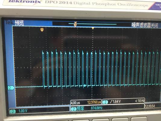
P2.6 SIMO signal.
Eric


