This thread has been locked.

If you have a related question, please click the "Ask a related question" button in the top right corner. The newly created question will be automatically linked to this question.

MSP430I2041: Disturbance after the crash, cannot be started

Part Number: MSP430I2041

We use the msp430i2041 in our products(thermostat), but there’s some problems in the use of this product .work crashed after a period of time, all IO don't have any output. It seems that CPU did not enter its working condition. The thermostat can run normally when just installed , but after running for a few days this problem occurred. Three such thermostats appeared this problem to a customer. We estimate that it is caused by the interference. The circuit is shown at the appended drawings, relatively simple. Interference is introduced only with power and analog input. Both the power and analog input are filtered (the power is added to the two-level filter, the analog input increases the capacitance), but crashes occur again, electricity to restart.Later we found by doing experiments, if we give the chip’s IO some interference (give high static impulses to JTAG ), the CPU crashes, all IO turn to input mode, but the WDT software is open. When interference disappeared, the CPU still cannot be started.
The other found a problem during the experiments, When external reset circuit is added to SP706 or not, if the voltage drop is not to zero, keeping at about 2.1V, then power it on, CPU can no longer start, the manual RST signal can not be restarted. It has to be Completely power off so the power can start. SP706 is less than 2.6V when the voltage is given RST low signal, CPU should enter the reset state, until the voltage meets the requirement.When given high voltage signal, CPU should start. But the CPU did not started, this is not absolutely.

    Please analyse the, what causes. What is the solution. Thank you very much!

Add: part of the code, the schematic diagram.

int __low_level_init(void)

{

unsigned long *jtagPwd = (unsigned long *)JTAG_DIS_PWD1;

/* Feed the watchdog timer */

WDTCTL = WDTPW | WDTCNTCL;

/* Check JTAG password locations and disable JTAG if passwords don't match.

* Else the JTAG will be enabled in the 64th cycle after reset.

*/

if ((*jtagPwd != 0x00000000) && (*jtagPwd != 0xFFFFFFFF))

{
/* Disable JTAG */

SYSJTAGDIS = JTAGDISKEY;
}

/* Calibration section

* Check for the BORIFG flag in IFG1. Execute calibration if this was a BORIFG.

* Else skip calibration

*/
if (IFG1 & BORIFG)
{
// Perform 2's complement checksum on 62 bytes of TLV data

unsigned int checksum = 0;

unsigned char *TLV_address_for_parse = ((unsigned char *)TLV_START);

unsigned int *TLV_address_for_checksum = ((unsigned int *)TLV_START + 1);
do
{
checksum ^= *TLV_address_for_checksum++;

} while (TLV_address_for_checksum <= (unsigned int *)TLV_END);

checksum ^= 0xFFFF;

checksum++;

// If check sum is not correct go to LPM4

if (*((unsigned int *)TLV_START) != checksum)

{

// Enter LPM4 if checksum failed

__bis_SR_register(LPM4_bits);

}

// Check sum matched, now set calibration values

//Calibrate REF

REFCAL1 = *(TLV_address_for_parse + TLV_CAL_REFCAL1);

REFCAL0 = *(TLV_address_for_parse + TLV_CAL_REFCAL0);

// Calibrate DCO

CSIRFCAL = *(TLV_address_for_parse + TLV_CAL_CSIRFCAL);

CSIRTCAL = *(TLV_address_for_parse + TLV_CAL_CSIRTCAL);

CSERFCAL = *(TLV_address_for_parse + TLV_CAL_CSERFCAL);

CSERTCAL = *(TLV_address_for_parse + TLV_CAL_CSERTCAL);

// Calibrate SD24

SD24TRIM = *(TLV_address_for_parse + TLV_CAL_SD24TRIM);

// Clear BORIFG

IFG1 &= ~(BORIFG);

}
/* Feed the watchdog timer */

WDTCTL = WDTPW | WDTCNTCL;

/* Return value:

* 1 - Perform data segment initialization.

* 0 - Skip data segment initialization.

*/

return 1;

}

void main(void)

{

static int adjustState=0;

u8 temp;

_DINT();

_NOP();

WDTCTL = WDTPW | WDTHOLD;// close WDT

CSCTL1 = DIVS__4 + DIVM__4; // MCLK=SMCLK=4096K

FCTL2 = FWKEY | FSSEL_1 |FN2 |FN3; // FN1 | FN3 |FN5; // MCLK/12 for Flash Timing Generator 257k~476K

// FCTL2 = FWKEY | FSSEL_1 |FN1 | FN3 |FN5; // MCLK/42 for Flash Timing Generator 257k~476K

WDTCTL=WDT_ARST_1000;

Init_TimerA0();

InitTimeA1Pwm();

InitCfg(); //congif init

Init_ADI(); //AD init

Init_485(); //UART init

_EINT();

while(1)

{

if(needRset==0)

WDTCTL=WDT_ARST_1000;

if((needInitAd==1)&&(CommSending()==0))

{

needInitAd=0;

_DINT();

Init_ADI(); //AD init

_EINT();

}

if(GetBeChanged()==YES)

{

DealData(0);

}

temp = GetKeyCode();

if(temp == KEY_SETUP_QQ)

{

SetRange(1);

adjustState = SET_RANGE1;

}

}

}

  • The first issue I notice is that Vcore capacitance is .1 uF when the datasheet states that it must be 470 nF. See if changing this value fixes the issue. The __low_level_init function does not need to be provided as it is standard for MSP430i2xx devices. You can test your design with a modified blink LED example to see if the issue lies with the hardware or software. If more code must be provided then please utilize the SyntaxHighlighter found when using rich formatting.

    Regards,
    Ryan
  • Today I change the Vcore capacitance of the circuit board to 470 nf and switch to the example program provided TI: blinking an LED code, after such modification the circuit board has a total of 4 pieces, 2 pieces found no cases of not working after power on(LED doesn't flash),but the other 2 pieces sometimes aren't working  (10% probability)after power on, then manually set to low level voltage cannot reset it(LED doesn't flash), must completely power off the electricity before it may be reset. At the same time I also did an experiment by adding the WDT chip SP706, for the two boards which can start normally still can normally start, but for the two boards which can not start properly, situation became worse, one of them is unable to start all the time, the possibility of the other not starting also increased. So in this case, the situation didn't improve by adding SP706.Please help me to analyze the reason and the solution

  • If the MSP430 still fails with the basic code then this verifies a power supply or hardware issue. Can you please capture some screenshots of VCC, VCORE, and RST lines during a disturbance which crashes the MCU? Are you able to share any PCB design files/images? The schematic closely matches that of MSP-TS430RHB32A but it would be good to run a continuity check to make sure all connections are as intended.

    Regards,
    Ryan
  • The schematic diagram is as follows. VCC is generated from the switch power supply, ac 220 v to 5 v, and use power chips for voltage stability after TPS77033.   The circuit board sometimes aren't working  (10% probability)after power on.Why?

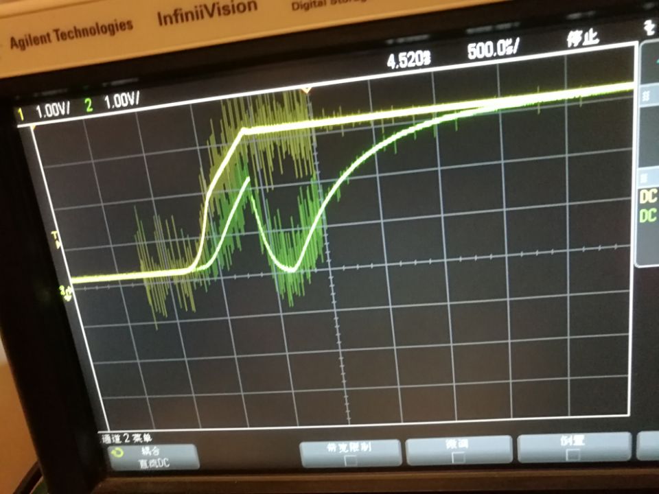
  •    this   waveforms of Vrst  VCC when working abnormally are shown ,VCC is yellow ,Vrst is green .
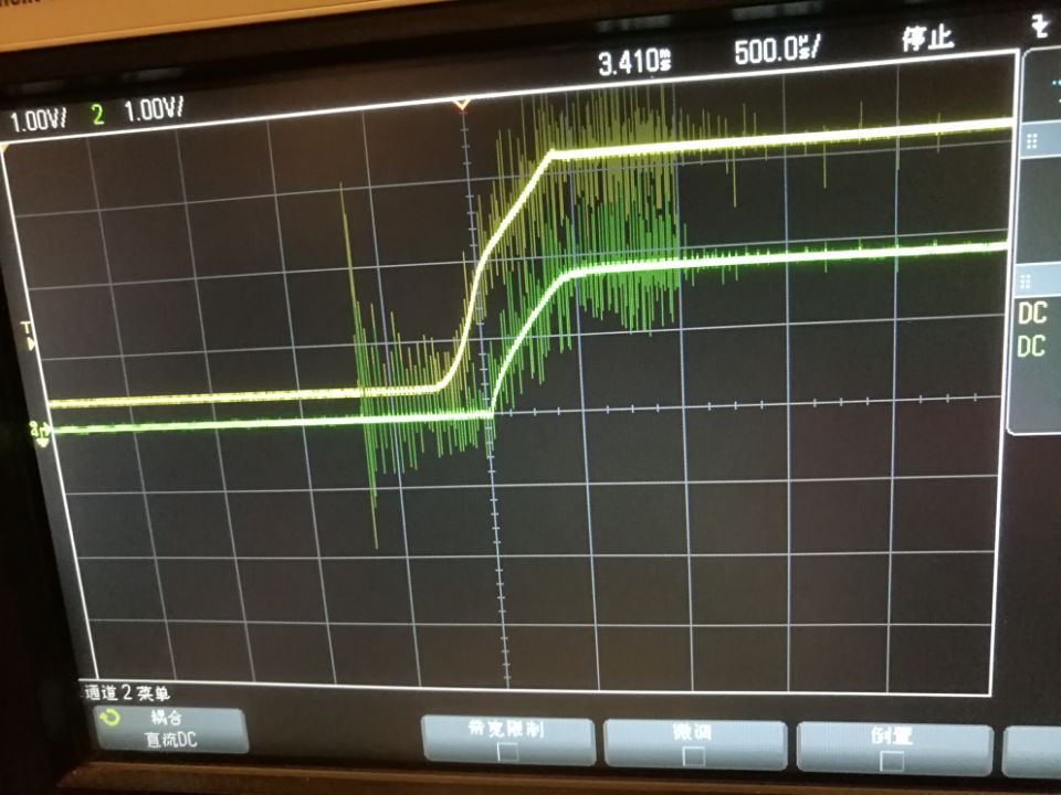
     this is VCC and Vcore ,Vcc is yellow ,Vcore is green.

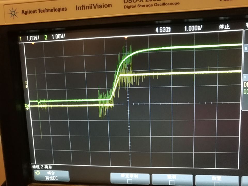
     this   waveforms of Vrst  VCC when working normally are shown ,VCC is yellow ,Vrst is green .

  • There does seem to be quite a bit of noise involved, such interference could be triggering the false reset event and preventing the PMM from releasing the MCU's BOR condition. What is the value of your pull-up resistor R11? Can you confirm that C15 (10 uF) is installed and located near the MSP430? Perhaps try to add more capacitance to the VCC rail to further control the voltage ramp-up.

    Regards,
    Ryan
  • the value of  pull-up resistor R11 is 47k,  I Can  confirm that C15 (10 uF) is installed and located near the MSP430.

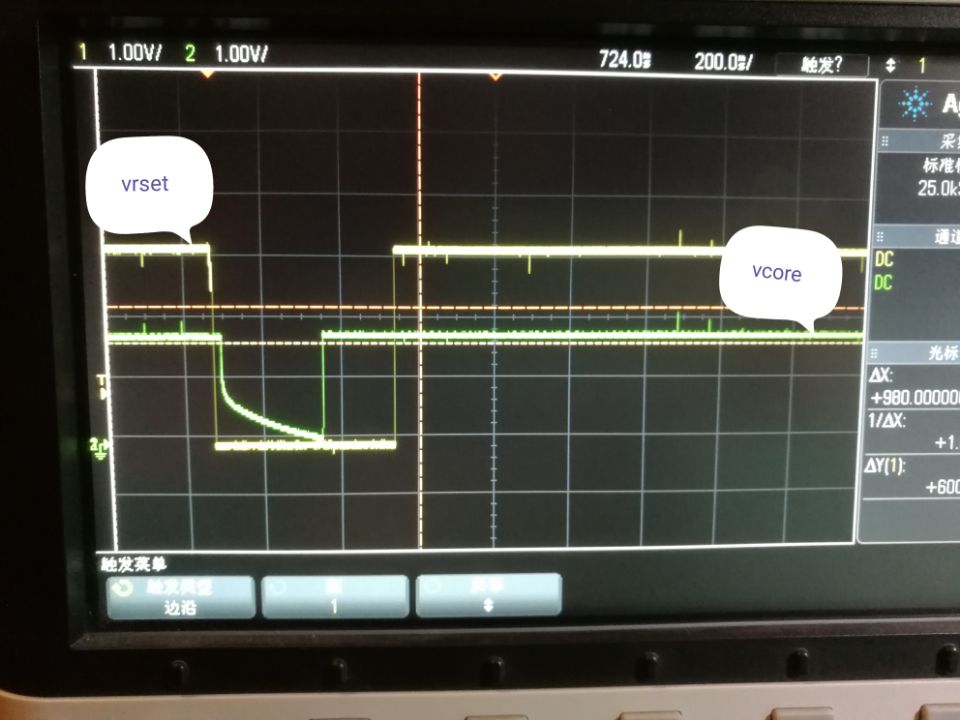
  • Today, I add WDT chip SP706 to the circuit and get the waveform after power on normally as follow:


    but when I frequently power on and power off, sometimes there's cases that the system can't start normally, the waveform that start abnormally is shown as follow:


    why is that this problem occurs, is this the original property of this chip? and is there any solution to this problem?  Thank you!

  • Hi

    Looks like signficant amount of current is consumed by the RST pin when it drops, can you measure current consumption in fail case and compare with good case while using the blinking LED example?

    Does any other GPIO see a voltage before the DVcc sees the 3.3V from the TPS circuitry? Very important to not back power the device via the ESD rails. If you are able simply disconnect all other pins of the device and do testing again.

    Does a serial resistor (e.g. 10 Ohm) help to filter the noise and make system more robust? Might help to check if it comes via DVCC or any ohter pin.
  • Hi,
    any update or progress on this thread?
  • The current is 4.7 mA,VCORE is 1.8V when frequently working, while the current is 1.0 mA and VCORE is 1.83V when it failed to start (using a flashing LED example).
    When it failed, the voltage of all IO ports is about 1.4 V. I disconnected all the pins on the CPU and got the same result.
    I added a resistor of 30 o in series at the front end of VCC. The problem of power failure was improved, but it was not completely solved.
    When the it failed to start, I powered off the CPU for 200mS (using SP706 chip to control), then tried to power it on but it was still unable to start, the test revealed the VCC powered off for 200 ms, but the VCORE’s power was still on .
  • Hi,

    when you mean you power off the device and Vcore is still there it means there is some backdoor supply right?

    So do you have any voltage applied to any pin when you power off DVCC? If yes than you will violate the specification which can lead to unpredictable behavior.

    Please read through:
    www.ti.com/lit/slaa530

  • I'm sorry. I got wrong with the problem about VCC losing power and Vcore not losing power.
    I have rewired the PCB, planting as many ground electrodes as possible around CPU. The distance between VCORE’s capacitance and the CPU is also the shortest. and the VCC of the CPU is added with 10uF’s capacitance. Currently, the test has not found that the power is not started. I would like to confirm whether the chip needs additional power management chip (such as SP706).

    Would you help me to check the below PCB wiring is reasonable, thank you!

  • The VCC, VCORE, VREF, and RST capacitors all share a single path to the minimal GND plane which could be a concern. There should not be a need for an external power management IC.

    Regards,
    Ryan
  • So this does not answer my question so I will repeat.

    If you power cylce you primary power is there any GPIO still powered during power up?
    Or in other words does any pin see any voltage during power up before DVCC sees the voltage?
  • I'm sorry. Regarding the VCC power off and VCORE power still on is my cause by measurement error. And the case is when the VCC power down VCORE also power down.

    Thank you!

  • We understand the measurement error and have disregarded this information, but when VCC and VCORE power down are there any GPIO pins still powered? Dietmar needs to know if any other pins have a voltage applied before DVCC on power up.

    Regards,
    Ryan

**Attention** This is a public forum