This thread has been locked.

If you have a related question, please click the "Ask a related question" button in the top right corner. The newly created question will be automatically linked to this question.

MSP430i2041: RIF of SD24 module

Part Number: MSP430I2041

Hello everybody,

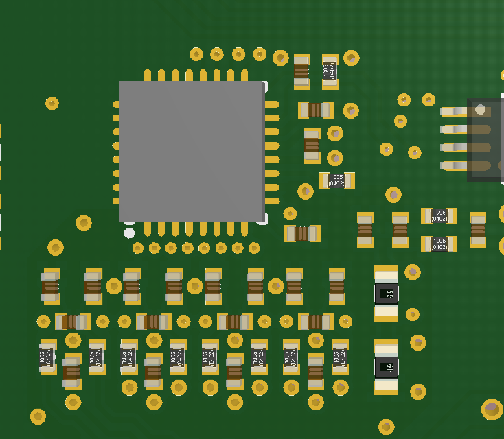
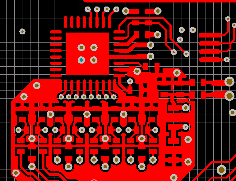
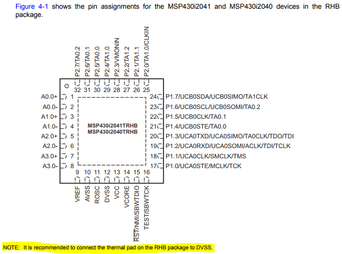
We are using an MSP430i2041RHB to measure some pressure sensor using the internal ADC (SD24). The ADC is operating in SD24GAINx = 16, i.e. the input range is around  /- 60mV using an external Vref at approx. 1.24V. All four channels are in use and are connected to the same type of sensor. Care has been taken so that all PCB lines to the inputs are symmetrical and shielded by AGND. AGND is split from the DGND plane and both are connected directly at the MSP430.

Everything works fine under normal operating conditions, but the design fails to pass RFI tests around 120-140MHz. Adding capacitors to improve immunity against difference and common-mode signals did not help at all. Even changing the input filter to reduce Fc to approx. 10Hz showed no improvement.

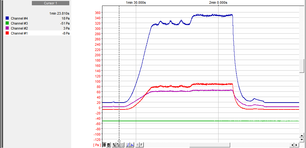
Interestingly enough, the problem shows on analog channels #1, #2 and #4, but not on channel #3. Reading the effected channels show voltages up to 11mV and the amplitude depends on the channel (channel #4 being the worst), but channel #3 does not show any error at all.


Any ideas what could be the reason for that effect?

  • Hello Robert,

    I'm looking into your request. In the meantime, can you please share screenshots of your schematic and PCB including the area around the SD24 inputs and the analog front end components?

    Regards,

    James

    MSP Customer Applications
  • Hello James,

    Thanks for your reply. I have tried to attach screen shots, but somehow failed. So this is the text part only and I will try to attach the screen shots in a later post.

    This is actually our second attempt to the PCB, after talking to the engineers at the EMC test laboratory. The PCB uses an eight layer stack with ground planes at both sides of the PCB (one below the top layer and the other above the bottom layer). Ground planes are split into DGND and AGND, with AGND being used in the analog input section only. And there are no digital signals running through the analog input section.

    Even so the PCB changed massively from the last attempt, there has been no change in RF immunity at all. Both hardware versions produce the following graphs (trying to attach in another post), as soon as the RF signal is turned on. The graphs are scaled to Pa with approx. 20uV / Pa, so channel #4 rises approx. by 6.6 mV while channel #3 does not show any error at all. Since the rework of the input section (filters and better trace layout) did not change anything, I am now under the impression that the RF signal has to enter the MSP430 somewhere else. I already suspected DGND, but that should effect all four channels in the same way, shouldn't it?

    Again, thank you very much for your reply. I am really out of ideas and any help is greatly appreciated.

  • This is a 3D view of the PCB (just to find your way around).

  • Top and mid layer. The mid layer runs the connection from the input filters to the analog input pins of the MSP430 and is AGND filled.

  • Ground planes and bottom layer. The bottom layer is filled by an AGND plane and runs SBWIO and SBWCK outside of the plane (and both signals are not connected while running the RF tests).

  • And there is the schematic.

  • This are the graphs of the ADC data.

  • Hello James,

    Just another fact I forget to share. The thermal pad of the RHB package is connected to DGND (DVSS). Maybe the RF signal noise gets picked up by the entire DGND plane and then gets coupled by the thermal pad to the bond wires. This could be the reason that channels are affected quite differently, if there is a significant difference in the length of the bond wires to the analog inputs of the die.

    But this is just a wild guess.

    Best regards,

    Robert

  • Hi Robert,

    Thank you very much for sharing all this information and the screenshots. It helps tremendously, especially for an issue and layout as complicated as this one.

    Looking at the connections from the input filters to the analog input pins of the MSP430, the routing seems to be similar and doesn't explain the differences observed on the various input channels. Also, since the rework of the input section (filters and better trace layout) did not change anything, I suspect that this area is not causing the issue.

    One possible cause for this issue would be if the analog traces are crossing between the AGND and DGND planes. During EMC tests, most problems are observed when traces are routed across a slot or a split in a ground or power plane. Since this routing causes both radiation and crosstalk issues, it is not recommended. Can you share a more zoomed-out screenshot of the Bottom Layer? I'm curious to know where the analog traces are coming from and that's not shown in the screenshot above.

    Another thing, I notice quite a few peninsulas in the AGND polygon on the Bottom Layer between the traces. If possible, I'd recommend removing them, since they can act like antennas and introduce additional noise.

    Also, are these four pressure sensors populated on the PCB or are they connected via wires? What happens if you disconnect or remove these sensors from the PCB and re-run the test - does it still fail?

    For your reference, I'm linking to some references below that discuss grounding techniques in mixed-signal systems. More specifically, it discusses the pros and cons for split and partitioned planes.

    Regards,

    James

    MSP Customer Applications

  • Robert Kindermann said:
    Just another fact I forget to share. The thermal pad of the RHB package is connected to DGND (DVSS).

    According to the datasheet, you're correctly connecting the thermal pad to DVSS (DGND).

    Regards,

    James

    MSP Customer Applications

  • Hi James,

    The analog traces to the pressure sensors run to the edge of the PCB and connect to another PCB which holds the sockets for the pressure sensors. Connection between both PCBs is done by an edge connector like the one found on DIMM memory modules. The bottom layer on the edge of the PCB looks like this:

    All polygons are done using the "Remove dead copper" option, so there should be no copper left that is not connected to AGND. Care has been taken that all signal traces have a valid return path, so no crossing of any voids in AGND of DGND (this is done even for signals that I assume to be low speed like the analog input traces). BTW, the first version of the PCB did not split AGND and DGND, so I would suspect that the split planes aren't the issue.

    The systems fails the RF tests regardless of the pressure sensor used. After looking at the graphs I suspected the pressure sensors at channel 1,2 and 4 to be the culprits. But nothing changed after swapping the sensors at channel 3 and 4. We even did tests without any sensor at channel 3 (ignoring the fact that open analog inputs aren't the best idea) and still channel 3 did not show any influence by the radio signal.

    The pressure sensors are similar to through hole ICs and are in fact located in an precision socket used for DIP ICs. There are no wires, just the pins of the pressure sensor. If the input filter is working as intended, I would assume that any high frequency RF noise picked up by the pressure sensor, the edge connector and the traces from the pressure sensor to the input filter get filtered there. Signals in the range of 120-140MHz should not be able to pass the filter and I think the noise somehow must get picked up after the input filter, i.e somewhere along the way from the input filter to the PGA inside the chip.

    Best regards,

    Robert

  • James, Robert,

    a lot of noise also sometimes is coupled via the supply planes itself. How is AVCC and DVCC, AVSS and DVSS connected?
    Where are the decoupling caps for the supply placed?
    Where is the RST pull up + cap placed?

    8 layers with a good GND plane sounds already very good?
    Did you ever simulated the PCB to see if somewhere radiates in the frequency range you see it failing during test?

    Also did you check following Apps Note which gives some basics regarding System Level ESD which is also good to consider for any EMC noise:
    www.ti.com/lit/slaa530
  • Hello Dietmar,

    Thank you very much for joining us. Well, here is the missing screen shot showing designators.

    C88 is the capacitor at reset, R81 the pull-up at reset, C86 the capacitor at Vcore, C89 the decoupling capacitor at DVcc. R80 connects Rosc to AGND (AVss) and C84 is the decoupling capacitor at Vref.

    The PCB uses an 8 layer stack-up: top layer - top ground (DGND plane) - mid layer 1 (signal layer) - power plane - mid layer 2 (signal layer) - mid layer 3 (signal layer) - bottom ground (DGND plane) - bottom layer. Both ground planes and the power plane are cut so that all analog signals reside over an AGND plane. The analog input traces from the input filters to the MSP430 run in mid layer 1, shielded by an AGND polygon.

    Splitting the ground plane into AGND and DGND planes is new with "version 2" of the PCB. The first attempt had a single ground plane and a completely different input section (none of the input trace were symmetrical or shielded by AGND). And there is no difference at all between both versions.

    I already considered noise at DGND and/or Vcc as possible reason. But I could not think of anything on those common pins to explain why channel 3 works perfect while the other three channels show major influence by the radio signal.

    We didn't do a simulation of the PCB. Actually, there is something strange to the frequency range the systems reacts upon. Any failure did show up between 100 and 140MHz, but the actual frequency has been different on different test days. First I thought this is due to the different PCBs tested (tolerance of the capacitors). But there is just one prototype of "version 2" and on one day the effect showed up between 136 and 139 MHz and on another day between 121 and 124MHz. The range is quite limited and shows really sharp edges, so that a change in frequency of 1MHz is enough to go from "no influence" to "offset by 6mV".

    Unfortunately, the graphs I have posted earlier are scaled to time (x-axis). But in fact everything left to the rising edge is just 1MHz below the failing frequency and shows no influence at all. Same holds true for the part right to the range. Once the frequency is just 1MHz above the error band, the influence is gone.

    And thanks for the application note, I will study that one.

    Best regards,

    Robert

  • Robert,

    I cannot see a very critical problem here. Caps are placed close and due to the GND and SUPPLY planes it seems to be properly connected to hold loop inductance low.
    And you're right why the channels behave different. If I understand it right channel 4 is the worst one right?

    Did you tried following things:
    1. Do not connect the sensors and short + and - terminal on all channels to measure the pure offset. Does it appear the same way?
    2. Did you tried to use internal Vref which is also 1.2V?
    3. Which conversion mode did you use? Group of channels or single channel? Can you change it from what you use at the moment and try again?

    Sorry for all the questions but the biggest mysterium is the difference in the channels therefore it would be interesting if the order when each channel converts makes a difference.
  • Dietmar,

    Yes, right, channel 4 is the worst one.

    The software is quite simple. Just sets up the SD24 and eUSCI_A0 module, then runs in a loop waiting for end of conversion and transmitting the results using the SPI of eUSCI_A0. SD24 is configured to convert a group of channels in continuous conversion mode (range is x16, OSR is 256). Inside the loop the interrupt flag of SD24CCTL3 is monitored to read all of the channels. Then LSBACC of all channels get reset and the results are read, all done from channel 1 to 4. Reading the conversion results looks something like this:

          if (SD24CCTL3 & SD24CCTL_SD24IFG)
            {
              SD24CCTL0 &= ~SD24CCTL_SD24LSBACC;
              SD24CCTL1 &= ~SD24CCTL_SD24LSBACC;
              SD24CCTL2 &= ~SD24CCTL_SD24LSBACC;
              SD24CCTL3 &= ~SD24CCTL_SD24LSBACC;

      sd24_read_cha_osr256 (&SD24MEM0, io_buf);
      sd24_read_cha_osr256 (&SD24MEM1, io_buf+2);
      sd24_read_cha_osr256 (&SD24MEM2, io_buf+4);
      sd24_read_cha_osr256 (&SD24MEM3, io_buf+6);
    }

    Again, I just can't see what this loop should make channel 3 "the chosen one".

    Dietmar Walther said:
    Did you tried following things:
    1. Do not connect the sensors and short + and - terminal on all channels to measure the pure offset. Does it appear the same way?
    2. Did you tried to use internal Vref which is also 1.2V?

    No, we didn't. The next test will be on Friday, 8th of September (hopefully). Then I will check, what happens if the channels are short circuit or internal Vref is used, And using single channel conversion.

    No worries about your questions. I really appreciate your help greatly.

    Best regards,

    Robert

  • Dietmar, James,

    I owe you an apology for causing all that trouble. But first things first. The MSP's SD24 is working perfectly, there is no influence by the applied RF signal whatsoever.

    In fact, the explanation to that strange behavior is so simple and so obvious, that I really feel ashamed having bothered you at all. Using Occam's razor in the first place would have helped. Obviously, the simplest explanation for any change in the pressure sensor's output signal is a change in the applied pressure of that sensor. And this is what actually happens, so there is no RF noise to be found on the conversion result. The conversion result shows nothing but valid sensor data.

    After two more testing days at the EMC laboratory and a third version of the PCB using a completely different ADC (ADS114S08IRHBT), we finally learned that some other part of the device picks up the RF signal and erroneously starts operating. That finally changes the pressure at three of the four pressure sensors and that's all there is.

    So please accept my apology, I am really sorry for the trouble.

    Again, the MSP430 works perfectly and the conversion results of the SD24 are great.

    Thank you so much for your support that is greatly appreciated.

    Best regards,

    Robert

    PS: You might want to mark that entire thread as completely unrelated to the MSP430 so no one gets irritated.

  • Robert,

    thanks a lot highly appreciated that you found the real root cause and shared your experience with us.
    For us it is very important that threads get succesfully closed!

    Believe once you found the root cause for a certain behavior it's always easy and obvious that's the way how we learn on daily base right.

    All the best for your future development!

  • Hello Robert,

    I echo what Dietmar expressed above. Thank you for the detailed explanation and for closing the loop on what you found. It's very helpful to our community, since others may face the same issue.

    Please let us know if you face any other issues.

    Regards,

    James

    MSP Customer Applications

**Attention** This is a public forum