Other Parts Discussed in Thread: MSP430F6736
Hi everyone
I have a measurement question relating to the I+/I- pins (ie pins 3&4) on the MSP430 that is being used in a power meter....

In the circuit above (note that this is the V+/V- inputs to the SD24B) points 3 and 4 are floating and not actually connected to the chip
The AC is 120V and voltage across 1&2=0.094V (This was predicted and measured) and voltage across 3&4=0.094V (this was also predicted and measured)
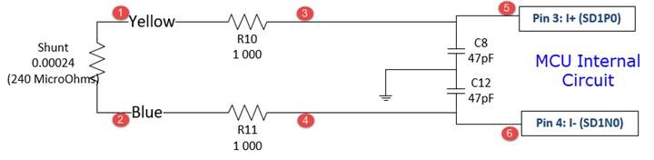
But now in the circuit above (note that this is now the I+/I- inputs to the SD24B) points 5 and 6 are floating and NOT actually connected to the chip...
The AC between AGND & LIVE (shunt) is 120V and the Load through the shunt is: 8.60A
Voltage across 1&2=2.081mV (This was predicted and measured)
Voltage across 3&4=4.6mv (measured)
Voltage across 5&6=4.6mv (measured)
And when disconnecting the Load (0A): Voltage across 5&6=4.0mv (measured)
And, since points 5 & 6 are not connected to the MCU, there is no current path.
So we now placed a 1K resistor across points 5 & 6 to complete a current path and we observed the following:
When Load: 0A Voltage across 5&6=1.3mv (measured)
When Load: 8.6A Voltage across 5&6=1.64mv (measured) The change compared to 0A is 26%.
And then we also replaced Capacitors C8 & C12 with 33nF (instead of the 47pF shown above) and observed the following:
When Load: 0A Voltage across 5&6=0.44v (measured)
When Load: 8.6A Voltage across 5&6=0.42v (measured) The change compared to 0A is now -4.5%.
So we can easily predict our inputs for (or rather the pd across) points 1 & 2 because the current loop is complete and the impact of the capacitors is minimal based on the given current flow.
However, this is not the case for points 5 & 6 (ie pins 3 & 4) which, it seems, are VERY sensitive to any noise.
And hence we need to know, or have a benchmark, of deliverable values to the MCU regarding Pins 3 & 4.
So NOW the questions...
In order to provide correct inputs for pins 3 & 4 (ie points 5 & 6 above) we would like to know:
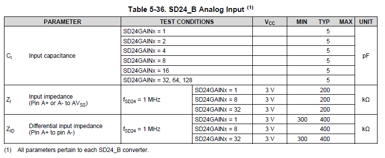
- What does the MCU's internal circuitry do at points 5 & 6 (ie pins 3 & 4) and what impact does it have when varying the capacitance values of C8 & C12?
- What is the recommended circuit configuration connecting the shunt to points 5 & 6 (ie to pins 3 & 4)?
- In order to filter out any noise effects, what is the benchmark measurements that we should aim towards for pins 3,4 and what is the recommendation for completing the current path (so as to emulate the MCU)?
thanks in advance