


Part Number: MSP430F2418
Other Parts Discussed in Thread: MSP430F235
We are occasionally seeing corruption of stored data on a Cypress FM24V10 FRAM chip interfaced to a MSP430F2418 MCU. We have contacted Cypress about the issue and they though it may be due to a timing issue on the I2C. Since the I2C bus master is the MSP430F2418, Cypress suggested opening a support request with TI as well.
The relevant part of the schematic is below:
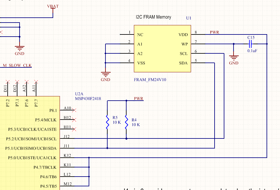
The FRAM chip is the only slave device connected to the I2C bus. The MSP 430 provides power to the bus and FRAM via 4 port pins. System power is provided by a 3.6V primary cell lithium battery.
Under normal operation, the FRAM chip is powered down when it is not in use. Periodically, the MSP430 powers on the FRAM and reads 4 bytes of data from address 0x0A on the FRAM chip due to a command generated from a user. Once the user command is serviced, the FRAM chip is powered down. After some time, the value stored at address 0x0A changes to a random value. No writes to that address are made and FRAM is non-volatile, so no change in the stored data is expected. Reads and writes to other addresses in FRAM (including adjacent addresses) do occur periodically.
To initialize and validate the data stored at address 0x0A, the MSP is interfaced to a computer via UCA1 in UART mode. The PC is able to issue commands to the MSP to read and write data to the FRAM. Furthermore, we have used a logic analyzer on the I2C bus to validate the MSP pass-through operation to/from the FRAM. Please note that during the failure (data corruption), the MSP is not connected to a PC.
We would like some of our units tested on a bench setup and a FA performed.
Typical I2C timing parameters as measured with a Tektronix MSO2014B scope:
Vcc good to bus start condition >700us
Bus stop to Vcc removal >50us
Vcc rise time 2.0us
Vcc fall time 2.4us
SCK frequency 235k
SCK rise time 666ns
SCK fall time <5ns
SCK high time 1.7us
SCK low time 2.0us
Vcc = FRAM chip power in above measurements
The MSP430 firmware's FRAM power control and read/write driver functions are provided below for reference. The IDE used is IAR workbench for MSP430 V6.50.4 with V7.4.2.4369 shared components. The generated .txt image was programmed to the test units with a TI gang programmer.
void FRAM_POWERON()
{
  // output low on SDA and SCL
  P5OUT &= ~(BIT1 | BIT2);
  P5DIR |= BIT1 | BIT2;
  P5SEL &= ~(BIT1 | BIT2);

#if __V1P2_HARDWARE__  ||  __V1P0_HARDWARE__           // 05/21/2017
  // 1.0 hardware FRAM power
  // 1.2 needs this as an output anyway to reduce power
  P2DIR |= BIT2; // P2.2 can power flash
  P2OUT |= BIT2; // output high to power FRAM (if S3 set to F_PWR)

  // 1.2 hardware FRAM power
  // 1.0 these are unused and need to be set as outputs anyway
  P5DIR &= ~BIT0;                  // set 5.0 to an input so that it does not fight P4 // 05/18/2017 // comment out 06/06/2017
  P4OUT |= BIT5 | BIT6 | BIT7;    // 05/18/2017 // comment out 06/06/2017
  P4DIR |= BIT5 | BIT6 | BIT7;
  P5OUT |= BIT0;                  // 05/18/2017 // comment out 06/06/2017
  P5DIR |= BIT0;                  // turn on P5.0 to help drive the memory // 05/18/2017


  // wait for power to stabalize
  _delay_us(700);
  // to avaoid a false start condition
  // set SDA high, then wait for it to settle
  P5OUT |= BIT1;
  _delay_us(5);
  // now output SCL high
  P5OUT |= BIT2;

  InitI2C();

#endif
}
void FRAM_POWEROFF()
{
  // output low on SCL to avoid a false start condition
  P5OUT &= ~(BIT2);
  P5DIR |= BIT2;
  P5SEL &= ~(BIT2);

#if __V1P2_HARDWARE__ ||  __V1P0_HARDWARE__           // 05/21/2017
  // 1.0 hardware FRAM power
  // 1.2 needs this as an output anyway to reduce power
  P2DIR |= BIT2;
  P2OUT &= ~BIT2;

  // 1.2 hardware FRAM power
  // 1.0 these are unused and need to be set as outputs anyway
  P5DIR &= ~BIT0;                     // set 5.0 to an input so that it does not fight P4 // 05/18/2017 // comment out 06/06/2017
  P4OUT &= ~(BIT5 | BIT6 | BIT7);    // 05/18/2017 // comment out 06/06/2017
  P5OUT &= ~BIT0;                    // 05/18/2017 // comment out 06/06/2017
  P5DIR |= BIT0;                     // turn on P5.0 to help drive the memory // 05/18/2017 // comment out 06/06/2017
#endif

  // turn off I2C pins
  /*
  P5OUT &= ~(BIT1 | BIT2);
  P5DIR |= BIT1 | BIT2;
  P5SEL &= ~(BIT1 | BIT2);
  */

  //UCSWRST=1: Enable Software Reset
  //UCB0TXIFG is set when UCSWRST =1 and I2C mode is selected. UCB0TXIE is reset when UCSWRST =1.
  //UCB0RXIFG and UCB0RXIE are reset when UCSWRST =1.
  UCB1CTL1 |= UCSWRST;


  // wait for power to stabalize
  _delay_us(100);
}

//---------------------------------------------------------------------------//
void InitI2C(void)
{
  //P3SEL = 0x06;             // P3.1 & P3.2 PORTS: select module function for the used I2C pins
  //P3DIR &= ~0x06;           // I/O pin direction set to INPUT

  P5SEL |= 0x06;             // P3.1 & P3.2 PORTS: select module function for the used I2C pins
  P5DIR &= ~0x06;           // I/O pin direction set to INPUT

  //Add Note: 12/22/2014
  //UCSWRST=1: Enable Software Reset
  //UCB0TXIFG is set when UCSWRST =1 and I2C mode is selected. UCB0TXIE is reset when UCSWRST =1.
  //UCB0RXIFG and UCB0RXIE are reset when UCSWRST =1.
  UCB1CTL1 |= UCSWRST;

  //Add Note: 12/22/2014
  //UCMST=1: Master; UCMODE=3: I2C; UCSYNC=1: Synchronous mode; UCSLA10=0: 7-bit addressing (slave);
  //UCA10=0: 7-bit addressing (master); UCMM =0: Single Master Environment
  UCB1CTL0 = (UCMST | UCMODE_3 | UCSYNC);

  //Add Note: 12/22/2014
  // UCSWRST=1: Enable Software Reset;  UCSSEL=3: USCI Clock source selects SMCLK
  // UCTR=0: Receiver; UCTXNACK=0: Acknowledge normally; UCTXSTP=0: No stop generated;
  // UCTXSTT=0: Do not generate START condition
  UCB1CTL1 = UCSWRST | UCSSEL_3;

  //Add Note: 12/22/2014
  //The BITCLK Frequency is given by f_BitClock = f_BRCLK/UCBR_X
  //UCB0BR0 (low byte): USCI_B0 Baud Rate Control Register 0 (low byte)
  //UCB0BR1 (high byte): USCI_B0 Baud Rate Control Register 1 (high byte)
  //  Bit clock prescaler setting: The 16-bit value of UCB0BR0 + UCB0BR1*256 forms the prescaler value.
  // UCB0BR0 = 4;                             // fSCL = SMCLK/4 = ~250kHz
  UCB1BR0 = 48;   //72                           //   SMCLK=8mhz
  UCB1BR1 = 0;                               //SMCLK/166KHz=48

  //Add Note: 12/22/2014
  // USCI_B0 I2C Slave Address Register: containing the slave address of the external device to be
  // addressed by the USCI_B0 module. It is only used in master mode. In 7-bit slave addressing mode,
  // bit 6 is the MST, and bits 9-7 are ignored.
  UCB1I2CSA = SlaveAddress;               // define Slave Address=0X50

  UCB1CTL1 &= ~UCSWRST;                   // Clear SW reset, resume operation
}

/* sendStop() -  provides a quick method to ensure a stop condition is made
                 on the I2C bus. Tries to create the stop for the set I2CTimeout
                 and returns TRUE if successfull.

  created 10/24/2017
*/
static int sendStop()
{
  unsigned int a;

  UCB0CTL1 |= UCTXSTP;                    // Send stop condition

  for (a = 0; a < I2CTimeout; ++a) // wait for stop to be sent
  {
    if ((UCB0CTL1 & UCTXSTP) == 0) break;
  }
  _delay_us(50); // ensure stop fully sent

  return a < I2CTimeout; // true if timeout not hit
}

//----------------------------------------------------------------------------
int LReadNbytesFromFRAM(int n, long faddr, unsigned char *p)  // use with 128K X 8 FRAM
{

  int     i;
  unsigned int a;
  union   {  long   x; unsigned char    b[4]; } u;


  if (!p)
  {

    return -1;
  }

  u.x = faddr;
  //UCB1CTL1 |= UCSWRST;                      // Clear SW reset, resume operation
  UCB1I2CSA = (SlaveAddress | u.b[2]);        // define Slave Address
  //UCB1CTL1 &= ~UCSWRST;                     // Clear SW reset, resume operation

  //while (UCB1CTL1 & UCTXSTP);             // Ensure stop condition got sent
  for (a = 0; a < I2CTimeout; ++a)
  {
    if ( !(UCB1CTL1 & UCTXSTP) ) break;    //UCTXSTP: Transmit STOP condition in master mode. Ignored in slave mode. //Add Note: 12/22/2014
  }

  if (a >= I2CTimeout)
  {

    return -2;
  }
  UCB1CTL1 |= UCTR;                        // set direction = write. UCTR=0: Receiver; UCTR=1: Transmitter. //Add Note: 12/22/2014
  UCB1CTL1 |= UCTXSTT;                     // I2C start condition. UCTXSTT=1: Transmit START condition in master mode. Ignored in salve mode.
  // sends Slave Adress w/direction & Start Flag //Add Note: 12/22/2014
  for (i = 0; i < 2; ++i)
  {
    //while (!(IFG2 & UCB0TXIFG));        // wait for xmit buffer empty
    for (a = 0; a < I2CTimeout; ++a)
    {

      if (UC1IFG & UCB1TXIFG) break;       //IFG2: Interrupt Flag Register 2  //Add Note: 12/22/2014
      //UCB0TXIFG: USCI_B0 transmit interrupt flag. It is set when UCB0TXBUF is empty.
    }

    if (a >= I2CTimeout)
    {

      sendStop(); // added 10/24/2017
      return -3;
    }
    //Add Note: 12/22/2014
    //UCB0TXBUF: it is the UCSI_B0 Transmit Buffer Register. The transmit data buffer is user accessible and holds the data
    // waiting to be moved into the transmit shift register and transmitted. Writing to the transmit data buffer clears UCB0TXIFG.
    UCB1TXBUF = u.b[i ^ 1];              // stuff txbuf with FRAM address byte (hi-lo)
  }

  //while (!(IFG2 & UCB0TXIFG));            // wait for xmit buffer empty
  for (a = 0; a < I2CTimeout; ++a)
  {
    if (UC1IFG & UCB1TXIFG) break;
  }

  if (a >= I2CTimeout)
  {

    sendStop(); // added 10/24/2017
    return -4;
  }
  //Add Note: 12/22/2014
  // UCB0RXBUF: it is the UCSI_B0 Receive Buffer Register. The receive-data buffer is user accessible
  // and contains the last received character from the receive shift register. Reading UCB0RXBUF
  // resets UCB0RXIFG.
  *p = UCB1RXBUF;                          // clear rx buffer full interrupt flag


  /************************************************************************************

  Insert an opcode ( Miscellaneous functions):  A synonym for __insert_opcode.
  _OPC(X) is defined as  __insert_opcode(X)

  void __insert_opcode(const unsigned op);

  Description:
  __insert_opcode inserts op into the code stream and can be used to insert special
  instructions directly into function code. op must be a compile-time constant.
  __insert_opcode is an intrinsic function and produces inline code.
  ************************************************************************************/
  // asm("   BIC.B #010h,&069h");           // set direction = read
  // asm("   BIS.B #002h,&069h");           // I2C start condition
  _OPC(0xc0f2);   //asm("   BIC.B #010h,&069h");   // set direction = read  <<<<<<<<<<<<<<<<<
  _OPC(0x0010);
  _OPC(0x00D9);
  _OPC(0xd3e2);   //asm("   BIS.B #002h,&069h");    // I2C start condition
  _OPC(0x00D9);

  --n;
  for (i = 0; i < n; ++i)                  // loop 1 less time than n-bytes requested
  {
    //while (!(IFG2 & UCB0RXIFG));        // wait for rx buffer full
    for (a = 0; a < I2CTimeout; ++a)
    {
      if (UC1IFG & UCB1RXIFG) break;      //UCB0RXIFG: USCI_B0 receive interrupt flag.
      //It is set when UCB0RXBUF has received a complete character.
    }

    if (a >= I2CTimeout)
    {

      sendStop(); // added 10/24/2017
      return -5;
    }
    *p++ = UCB1RXBUF;                   // stuff *p++ with rxbuf
  }

  UCB1CTL1 |= UCTXSTP;                    // Send stop condition

  //while (!(IFG2 & UCB0RXIFG));            // wait for rx buffer full
  for (a = 0; a < I2CTimeout; ++a)
  {
    if (UC1IFG & UCB1RXIFG) break;
  }

  if (a >= I2CTimeout)
  {

	sendStop(); // added 10/24/2017
    return -6;
  }
  *p++ = UCB1RXBUF;                       // stuff *p++ with last byte from rxbuf

  for (a = 0; a < I2CTimeout; ++a) // wait for stop to be sent
  {
    if ((UCB1CTL1 & UCTXSTP) == 0) break;
  }
  _delay_us(50); // ensure stop fully sent


  return (++n);                           // return with
}

//---------------------------------------------------------------------------
int LWriteNbytesToFRAM(int n, long faddr, unsigned char *p)  // use with 128K X 8 FRAM
{
  //FRAM_POWERON(); //COMMENT OUT 05/18/2017 // 06/06/2017
  int     i;
  unsigned int a; // changed a to unsigned int from int
  union   { long   x; unsigned char    b[4]; } u;

  if(faddr <= 10)
  {
    u.x = faddr;    // 05/21/2017
  }

  if (!p)
  {

    return -1;
  }
  u.x = faddr;

  //UCB1CTL1 |= UCSWRST;                    // Clear SW reset, resume operation
  UCB1I2CSA = (SlaveAddress | u.b[2]);      // define Slave Address
  //UCB1CTL1 &= ~UCSWRST;                   // Clear SW reset, resume operation

  //while (UCB1CTL1 & UCTXSTP);             // Ensure stop condition got sent
  for (a = 0; a < I2CTimeout; ++a)
  {
    if ( !(UCB1CTL1 & UCTXSTP) ) break;
  }

  if (a == I2CTimeout)
  {

    return -1;
  }

  UCB1CTL1 |= UCTR;                         // set direction = write
  UCB1CTL1 |= UCTXSTT;                      // I2C start condition
  // sends Slave Adress w/direction & Start Flag
  for (i = 0; i < 2; ++i)
  {
    //while (!(IFG2 & UCB0TXIFG));        // wait for xmit buffer empty
    for (a = 0; a < I2CTimeout; ++a)
    {
      if (UC1IFG & UCB1TXIFG) break;
    }

    if (a == I2CTimeout)
    {

      sendStop(); // added 10/24/2017
      return -1;
    }

    UCB1TXBUF = u.b[i ^ 1];               // stuff txbuf with FRAM address byte (hi-lo)
  }

  for (i = 0; i < n; ++i)
  {
    //while (!(IFG2 & UCB0TXIFG));       // wait for xmit buffer empty
    for (a = 0; a < I2CTimeout; ++a)
    {
      if (UC1IFG & UCB1TXIFG) break;
    }

    if (a == I2CTimeout)
    {

      sendStop(); // added 10/24/2017
      return -1;
    }

    UCB1TXBUF = *(p++);                  // stuff rxbuf with *p++
  }

  //while (!(IFG2 & UCB0TXIFG));          // wait for xmit buffer empty
  for (a = 0; a < I2CTimeout; ++a)
  {
    if (UC1IFG & UCB1TXIFG) break;
  }

  if (a == I2CTimeout)
  {

    sendStop(); // added 10/24/2017
    return -1;
  }

  UCB1CTL1 |= UCTXSTP;                    // Send stop condition


  for (a = 0; a < I2CTimeout; ++a) // wait for stop to be sent
  {
    if ((UCB1CTL1 & UCTXSTP) == 0) break;
  }
  _delay_us(50); // ensure stop fully sent

  return (n);
}


//This function is exactly same as LReadNbytesFromFRAM(), but no power on/off control.
//This must be called only from TAM_Read (case 0x05) to read the FRAM config contents
int LReadNbytesFromFRAM_CFG(int n, long faddr, unsigned char *p)  // use with 128K X 8 FRAM
{
  int     i;
  unsigned int a;
  union   {  long   x; unsigned char    b[4]; } u;


  if (!p)
  {

    return -1;
  }
  u.x = faddr;

  //UCB1CTL1 |= UCSWRST;                      // Clear SW reset, resume operation
  UCB1I2CSA = (SlaveAddress | u.b[2]);        // define Slave Address
  //UCB1CTL1 &= ~UCSWRST;                     // Clear SW reset, resume operation

  //while (UCB1CTL1 & UCTXSTP);             // Ensure stop condition got sent
  for (a = 0; a < I2CTimeout; ++a)
  {
    if ( !(UCB1CTL1 & UCTXSTP) ) break;    //UCTXSTP: Transmit STOP condition in master mode. Ignored in slave mode. //Add Note: 12/22/2014
  }

  if (a >= I2CTimeout)
  {

    return -2;
  }
  UCB1CTL1 |= UCTR;                        // set direction = write. UCTR=0: Receiver; UCTR=1: Transmitter. //Add Note: 12/22/2014
  UCB1CTL1 |= UCTXSTT;                     // I2C start condition. UCTXSTT=1: Transmit START condition in master mode. Ignored in salve mode.
  // sends Slave Adress w/direction & Start Flag //Add Note: 12/22/2014
  for (i = 0; i < 2; ++i)
  {
    //while (!(IFG2 & UCB0TXIFG));        // wait for xmit buffer empty
    for (a = 0; a < I2CTimeout; ++a)
    {

      if (UC1IFG & UCB1TXIFG) break;       //IFG2: Interrupt Flag Register 2  //Add Note: 12/22/2014
      //UCB0TXIFG: USCI_B0 transmit interrupt flag. It is set when UCB0TXBUF is empty.
    }

    if (a >= I2CTimeout)
    {

      sendStop(); // added 10/24/2017
      return -3;
    }
    //Add Note: 12/22/2014
    //UCB0TXBUF: it is the UCSI_B0 Transmit Buffer Register. The transmit data buffer is user accessible and holds the data
    // waiting to be moved into the transmit shift register and transmitted. Writing to the transmit data buffer clears UCB0TXIFG.
    UCB1TXBUF = u.b[i ^ 1];              // stuff txbuf with FRAM address byte (hi-lo)
  }

  //while (!(IFG2 & UCB0TXIFG));            // wait for xmit buffer empty
  for (a = 0; a < I2CTimeout; ++a)
  {
    if (UC1IFG & UCB1TXIFG) break;
  }

  if (a >= I2CTimeout)
  {

    sendStop(); // added 10/24/2017
    return -4;
  }
  //Add Note: 12/22/2014
  // UCB0RXBUF: it is the UCSI_B0 Receive Buffer Register. The receive-data buffer is user accessible
  // and contains the last received character from the receive shift register. Reading UCB0RXBUF
  // resets UCB0RXIFG.
  *p = UCB1RXBUF;                          // clear rx buffer full interrupt flag


  /************************************************************************************

  Insert an opcode ( Miscellaneous functions):  A synonym for __insert_opcode.
  _OPC(X) is defined as  __insert_opcode(X)

  void __insert_opcode(const unsigned op);

  Description:
  __insert_opcode inserts op into the code stream and can be used to insert special
  instructions directly into function code. op must be a compile-time constant.
  __insert_opcode is an intrinsic function and produces inline code.
  ************************************************************************************/
  // asm("   BIC.B #010h,&069h");           // set direction = read
  // asm("   BIS.B #002h,&069h");           // I2C start condition
  _OPC(0xc0f2);   //asm("   BIC.B #010h,&069h");   // set direction = read  <<<<<<<<<<<<<<<<<
  _OPC(0x0010);
  _OPC(0x00D9);
  _OPC(0xd3e2);   //asm("   BIS.B #002h,&069h");    // I2C start condition
  _OPC(0x00D9);

  --n;
  for (i = 0; i < n; ++i)                  // loop 1 less time than n-bytes requested
  {
    //while (!(IFG2 & UCB0RXIFG));        // wait for rx buffer full
    for (a = 0; a < I2CTimeout; ++a)
    {
      if (UC1IFG & UCB1RXIFG) break;      //UCB0RXIFG: USCI_B0 receive interrupt flag.
      //It is set when UCB0RXBUF has received a complete character.
    }

    if (a >= I2CTimeout)
    {

      sendStop(); // added 10/24/2017
      return -5;
    }
    *p++ = UCB1RXBUF;                   // stuff *p++ with rxbuf
  }

  UCB1CTL1 |= UCTXSTP;                    // Send stop condition

  //while (!(IFG2 & UCB0RXIFG));            // wait for rx buffer full
  for (a = 0; a < I2CTimeout; ++a)
  {
    if (UC1IFG & UCB1RXIFG) break;
  }

  if (a >= I2CTimeout)
  {

    sendStop(); // added 10/24/2017
    return -6;
  }
  *p++ = UCB1RXBUF;                       // stuff *p++ with last byte from rxbuf

  for (a = 0; a < I2CTimeout; ++a) // wait for stop to be sent
  {
    if ((UCB1CTL1 & UCTXSTP) == 0) break;
  }
  _delay_us(50); // ensure stop fully sent

  return (++n);                           // return with
}


//---------------------------------------------------------------------------
int SetFRAMArea(int n, long faddr,unsigned char Data)  // use with 128K X 8 FRAM
{
  //FRAM_POWERON(); //COMMENT OUT 05/18/2017 // 06/06/2017
  int     i;
  unsigned int a; // changed a from int to unsigned int 10/24/2017
  union   { long   x; unsigned char    b[4]; } u;

  u.x = faddr;

  //UCB1CTL1 |= UCSWRST;                    // Clear SW reset, resume operation
  UCB1I2CSA = (SlaveAddress | u.b[2]);      // define Slave Address
  //UCB1CTL1 &= ~UCSWRST;                   // Clear SW reset, resume operation

  //while (UCB1CTL1 & UCTXSTP);             // Ensure stop condition got sent
  for (a = 0; a < I2CTimeout; ++a)
  {
    if ( !(UCB1CTL1 & UCTXSTP) ) break;
  }

  if (a == I2CTimeout)
  {

    return -1;
  }


  UCB1CTL1 |= UCTR;                         // set direction = write
  UCB1CTL1 |= UCTXSTT;                      // I2C start condition
  // sends Slave Adress w/direction & Start Flag
  for (i = 0; i < 2; ++i)
  {
    //while (!(IFG2 & UCB0TXIFG));        // wait for xmit buffer empty
    for (a = 0; a < I2CTimeout; ++a)
    {
      if (UC1IFG & UCB1TXIFG) break;
    }

    if (a == I2CTimeout)
    {

      sendStop(); // added 10/24/2017
      return -1;
    }


    UCB1TXBUF = u.b[i ^ 1];               // stuff txbuf with FRAM address byte (hi-lo)
  }

  for (i = 0; i < n; ++i)
  {
    //while (!(IFG2 & UCB0TXIFG));       // wait for xmit buffer empty
    for (a = 0; a < I2CTimeout; ++a)
    {
      if (UC1IFG & UCB1TXIFG) break;
    }

    if (a == I2CTimeout)
    {

      sendStop(); // added 10/24/2017
      return -1;
    }


    UCB1TXBUF = Data;                  // write 0 to clear memory
  }

  //while (!(IFG2 & UCB0TXIFG));          // wait for xmit buffer empty
  for (a = 0; a < I2CTimeout; ++a)
  {
    if (UC1IFG & UCB1TXIFG) break;
  }

  if (a == I2CTimeout)
  {

    sendStop(); // added 10/24/2017
    return -1;
  }


  UCB1CTL1 |= UCTXSTP;                    // Send stop condition


  for (a = 0; a < I2CTimeout; ++a) // wait for stop to be sent
  {
    if ((UCB1CTL1 & UCTXSTP) == 0) break;
  }
  _delay_us(50); // ensure stop fully sent

  return (n);
}


