This thread has been locked.

If you have a related question, please click the "Ask a related question" button in the top right corner. The newly created question will be automatically linked to this question.

CCS/MSP430FR5969: MSP430FR5969

Part Number: MSP430FR5969
Other Parts Discussed in Thread: MSP-EXP430FR5969,

Tool/software: Code Composer Studio

Dear all,

I'm testing SPI interface between MSP430 and the UHF RFID IC Tag SL900A. The problem is that: I cannot write/read data to/from SL900A. And there is a big problem regarding hardware. I don't know why. Please help me in this regard. Thank you so much.

1) Hardware setup:
* MSP430: I'm using MSP-EXP430FR5969. and eUSCI_A1 SPI module: P2.4: UCA1CLK (32 kHz); P2.5: UCA1SIMO; P2.6: UCA1SOMI; MCU operates with CLK = 1MHz
* SL900A: as below, except pin 2 is connected to pin 8 (recommended in page 3 datasheet). Battery is 2.5V (but MCU is connected directly to computer through USB, so 2 different Vcc for SL900A & MCU).

2) Coding:

#include <msp430.h>

volatile unsigned char RXData = 0;
volatile unsigned char TXData;
volatile unsigned char var=0;
volatile unsigned int count=0;

int main(void)
{
WDTCTL = WDTPW | WDTHOLD; // Stop watchdog timer

// Configure GPIO
P2SEL1 |= BIT4; // USCI_A1 operation
P2SEL1 |= BIT5 | BIT6; // USCI_A1 operation
PJSEL0 |= BIT4 | BIT5; // For XT1

P1DIR |= BIT4 + BIT0;
// Disable the GPIO power-on default high-impedance mode to activate
// previously configured port settings
PM5CTL0 &= ~LOCKLPM5;

// XT1 Setup
CSCTL0_H = CSKEY >> 8; // Unlock CS registers
CSCTL1 = DCOFSEL_0; // Set DCO to 1MHz
CSCTL2 = SELA__LFXTCLK | SELS__DCOCLK | SELM__DCOCLK;
CSCTL3 = DIVA__1 | DIVS__1 | DIVM__1; // set all dividers
CSCTL4 &= ~LFXTOFF;
do
{
CSCTL5 &= ~LFXTOFFG; // Clear XT1 fault flag
SFRIFG1 &= ~OFIFG;
}while (SFRIFG1&OFIFG); // Test oscillator fault flag
CSCTL0_H = 0; // Lock CS registers

// Configure USCI_A0 for SPI operation
UCA1CTLW0 = UCSWRST; // **Put state machine in reset**
UCA1CTLW0 |= UCMST | UCSYNC | UCMSB; // 3-pin, 8-bit SPI master, MSB first
// Clock polarity: data changed with first low-to-high transition of CLK
UCA1CTLW0 |= UCSSEL__ACLK; // ACLK
UCA1BR0 = 0x00; // fclk = 32kHz
UCA1BR1 = 0; //
UCA1MCTLW = 0; // No modulation
UCA1CTLW0 &= ~UCSWRST; // **Initialize USCI state machine**
//UCA1IE |= UCRXIE; // Enable USCI_A0 RX interrupt

P1OUT |= BIT4; // SEN is enabled
_delay_cycles(200);

while(1)
{
UCA1IE |= UCTXIE;
__bis_SR_register(LPM0_bits | GIE); // CPU off, enable interrupts

__delay_cycles(2000); // Delay before next transmission
P1OUT ^= BIT0;
}
}

#if defined(__TI_COMPILER_VERSION__) || defined(__IAR_SYSTEMS_ICC__)
#pragma vector=USCI_A1_VECTOR
__interrupt void USCI_A1_ISR(void)
#elif defined(__GNUC__)
void __attribute__ ((interrupt(USCI_A1_VECTOR))) USCI_A1_ISR (void)
#else
#error Compiler not supported!
#endif
{
switch(__even_in_range(UCA1IV, USCI_SPI_UCTXIFG))
{
case USCI_NONE: break;
case USCI_SPI_UCRXIFG:
RXData = UCA1RXBUF;
UCA1IFG &= ~UCRXIFG;
__bic_SR_register_on_exit(LPM0_bits); // Wake up to setup next TX
break;
case USCI_SPI_UCTXIFG:
count++;
if (var==0) {
TXData = 0;
UCA1TXBUF = TXData; // Transmit characters
var++;
}
else if (var ==1) {
TXData = 0x64;
UCA1TXBUF = TXData; // Transmit characters
var++;
}
else if (var == 2) {
TXData = 0x55;
UCA1TXBUF = TXData; // Transmit characters
var++;
}
UCA1IE &= ~UCTXIE;
__bic_SR_register_on_exit(LPM0_bits); // Wake up to setup next TX

break;
default: break;
}
}

3) Problems:

* Reading: when I tried to read data from FIFO (using Direct Command), I got only noise. Please see the pic below, when (1): SPI CLK, (2): P2.6 (UCA1SOMI). One more thing: I had to disconnect GND between SL900A and MCU. If their GNDs were connected, I got NO CLK (only spike instead of bit0-1).

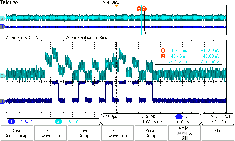
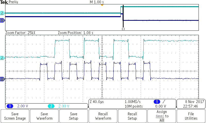
* Writing: I tried to write data (0x55) into User's Memory of SL900A, started at addr of 0x064. These are 3 bytes I wrote to SL900A. But then, the data were all 0 when I read User Memory from reader (RFID interface).
(1): SPI CLK; (2): P2.5 (UCA1SIMO)

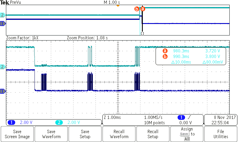
Byte 1: 0x00 (Write Command)


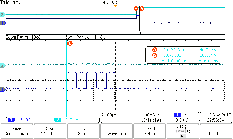
Byte 2: 0x64 (Address of SL900A EEPROM)

Byte 3: 0x55 (Data to be written)


I'm so confused. Please help me explain these things. Thank you so much.

  • Minh,

    You are operating outside of the recommended communication operating condition of VCC +/- 0.3 V at each pin, since the MSP430 is 3.3 V and the SL900A is 2.5 V. Your code did not attach correctly but you will need to make sure that the clock phase and polarity settings are aligned between the two devices, although it appears to be correct from the screenshots. I notice that the CS pin should also be active high. Make sure to refer to the MSP430FR5969 SPI examples as well as any SL900A resources you might have found.

    Regards,
    Ryan
  • Dear Ryan,

    Thank you so much for your response. Here is my coding. Yes the CS (SEN pin in SL900A case) was active high throughout the transaction. The Clock polarity is configured: UCCKPH = UCCKPL = 0, so that the data will be changed on the 1st rising edge of each CLK, fit with SL900A timing (plz refer to the pic below).

    ======Coding=======

    #include <msp430.h>

    volatile unsigned char RXData = 0;
    volatile unsigned char TXData;
    volatile unsigned char var=0;
    volatile unsigned int count=0;

    int main(void)
    {
    WDTCTL = WDTPW | WDTHOLD; // Stop watchdog timer

    // Configure GPIO
    P2SEL1 |= BIT4; // USCI_A1 operation
    P2SEL1 |= BIT5 | BIT6; // USCI_A1 operation
    PJSEL0 |= BIT4 | BIT5; // For XT1

    P1DIR |= BIT4 + BIT0;
    // Disable the GPIO power-on default high-impedance mode to activate
    // previously configured port settings
    PM5CTL0 &= ~LOCKLPM5;

    // XT1 Setup
    CSCTL0_H = CSKEY >> 8; // Unlock CS registers
    CSCTL1 = DCOFSEL_0; // Set DCO to 1MHz
    CSCTL2 = SELA__LFXTCLK | SELS__DCOCLK | SELM__DCOCLK;
    CSCTL3 = DIVA__1 | DIVS__1 | DIVM__1; // set all dividers
    CSCTL4 &= ~LFXTOFF;
    do
    {
    CSCTL5 &= ~LFXTOFFG; // Clear XT1 fault flag
    SFRIFG1 &= ~OFIFG;
    }while (SFRIFG1&OFIFG); // Test oscillator fault flag
    CSCTL0_H = 0; // Lock CS registers

    // Configure USCI_A0 for SPI operation
    UCA1CTLW0 = UCSWRST; // **Put state machine in reset**
    UCA1CTLW0 |= UCMST | UCSYNC | UCMSB; // 3-pin, 8-bit SPI master, MSB first
    // Clock polarity: data changed with first low-to-high transition of CLK
    UCA1CTLW0 |= UCSSEL__ACLK; // ACLK
    UCA1BR0 = 0x00; // fclk = 32kHz
    UCA1BR1 = 0; //
    UCA1MCTLW = 0; // No modulation
    UCA1CTLW0 &= ~UCSWRST; // **Initialize USCI state machine**
    //UCA1IE |= UCRXIE; // Enable USCI_A0 RX interrupt

    P1OUT |= BIT4;
    _delay_cycles(200);

    while(1)
    {
    UCA1IE |= UCTXIE;
    __bis_SR_register(LPM0_bits | GIE); // CPU off, enable interrupts

    __delay_cycles(2000); // Delay before next transmission
    P1OUT ^= BIT0;
    }
    }

    #if defined(__TI_COMPILER_VERSION__) || defined(__IAR_SYSTEMS_ICC__)
    #pragma vector=USCI_A1_VECTOR
    __interrupt void USCI_A1_ISR(void)
    #elif defined(__GNUC__)
    void __attribute__ ((interrupt(USCI_A1_VECTOR))) USCI_A1_ISR (void)
    #else
    #error Compiler not supported!
    #endif
    {
    switch(__even_in_range(UCA1IV, USCI_SPI_UCTXIFG))
    {
    case USCI_NONE: break;
    case USCI_SPI_UCRXIFG:
    RXData = UCA1RXBUF;
    UCA1IFG &= ~UCRXIFG;
    __bic_SR_register_on_exit(LPM0_bits); // Wake up to setup next TX
    break;
    case USCI_SPI_UCTXIFG:
    count++;
    if (var==0) {
    TXData = 0;
    UCA1TXBUF = TXData; // Transmit characters
    var++;
    }
    else if (var ==1) {
    TXData = 0x64;
    UCA1TXBUF = TXData; // Transmit characters
    var++;
    }
    else if (var == 2) {
    TXData = 0x55;
    UCA1TXBUF = TXData; // Transmit characters
    var++;
    }
    UCA1IE &= ~UCTXIE;
    __bic_SR_register_on_exit(LPM0_bits); // Wake up to setup next TX

    break;
    default: break;
    }
    }

    I don't know where I did wrong. Thank you for any suggestion TT_TT

  • Hello Minh,

    Your SPI initialization appears fine, pretty much directly copied from a code example. But you still need to address the voltage difference issue of your hardware setup. There also may be more information found upon further reading of the SL900A datasheet.

    Regards,
    Ryan
  • Hi Ryan,

    Thank you for your comment. I found out the problem of hardware. It was because pin VBAT (pin 13) of SL900A was connected to other "empty" ICs (the IC place  but no IC there) that I could not control. So I cut the connection of VBAT with other ICs, and now the voltage levels are correct. One battery for both MCU and SL900A and no more strange logic levels.

    However I still could not write/read data into/from SL900A. In SPI WRITE mode, I observed no "ACK" (the high pulse in DOUT) after all data have been transmitted as illustrated in chip datasheet:

    There might be some reasons for this problem:

    - SPI CLK is too low ? (32KHz) Datasheet shows no minimum SPI CLK, just the upper bound (1-2MHz)

    - SEN pin is not deactivated after transmission has finished --> I tested this already. It caused no change, i.e. no data has been written into SL900A even SEN was been deactivated after writing. 

    - Some delay after writing?  --> I put 10ms after each Tx (3 bytes in my case: 0x00 --> WRITE mode, 0x64 --> physical address of SL900A USER's memory, 0x18 --> data to be written). 

    Still not working TT_TT

    Btw: I'm using another account. It's still me the author.

  • Hi Minh,

    Feel free to adjust the SPI CLK frequency and delay timing. This forum's focus is on MSP430 issues but your problems appear to center around the SL900A. I can say that one would typically poll the TXIFG flag instead of using interrupts in the manner with which your code operates, however this is not the cause of the difficulties you are experiencing.

    Regards,
    Ryan
  • Hi Ryan,

    Thank you for your suggestion. I'll try this. I'm using interrupt because my application requires power saving, a lot. 

    By the way, could you please explain more about how LPM operates in MSP430? As I understand, right after entering LMP with the command __bis_SR_register(LPM0_bits | GIE), all commands afterwards (in main loop) will not be executed until the __bic_SR_register_on_exit(LPM0_bits) command is executed.

    - If there is no  __bic_SR_register_on_exit(LPM0_bits) command during an interrupt service routine, after returning from interrupt service routine, the device will sleep again, waiting right at the __bis_SR_register(LPM0_bits | GIE command? I mean no other commands in main loop will be executed?

    - So, if other interrupt conditions occur, the interrupt service routine will be implemented many times, again and again. The device never exits LPM, Main loop always waits at the entering LPM command as shown above.

    Am I right? Thank you for any explanation. 

  • Yes Minh, your analysis of LPM execution is correct.

    Regards,
    Ryan
  • Updated:

    Thank you very much for your time. I've finally solved the problems and SL900A has worked. The problem were about SPI interface. I had not recognized for SPI reading, I have to write dummy bytes in order to receive data. So I fixed my coding and it worked :)

**Attention** This is a public forum