This thread has been locked.

If you have a related question, please click the "Ask a related question" button in the top right corner. The newly created question will be automatically linked to this question.

CCS/MSP430FR5969: Assembly language: cycles to execute instructions

Part Number: MSP430FR5969
Other Parts Discussed in Thread: MSP-EXP430FR5969

Tool/software: Code Composer Studio

Dear all,

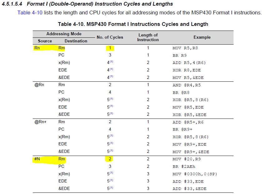
I'm working with assembly language and need to calculate exact timing for my coding. I do not see the difference between these codes, but according to the author they take different cycles to operate

	MOV		#dataBuf,	R12		                ;[2] load the &dataBuf[0]
	MOV		#DATABUFF_SIZE,	R13		;[1] load into corr reg (numBytes)
MOV #TX_TIMING_ACK, R5 ;[2]

whereas dataBuf is declared as uint8_t dataBuf[30], DATABUFF_SIZE and TX_TIMING_ACK are defined as constants. The numbers in [] are the number of cycles for the codes to execute. 

I found the Instruction Set Summary from TI. But I got so confused from the sample project I'm reading as above mentioned.

Thank you for any advice. 

  • What are the values of DATABUFF_SIZE and TX_TIMING_ACK? If these values come from the constant generator, you save ony cycle.

    And you should ask the author.
  • Hi Minh,

    all three instructions write a constant to a register which takes 2 cycles as can be seen in Section 4.5.1.5.4 of the User's Guide (slau367n). In case of the second instruction it seams to be possible to replace the constant #DATABUFF_SIZE with a constant from the Constant Generator (R3 & R4). In this case the data is written from one register to another which only takes 1 cycle.

    Thanks and best regards
    Christoph

  • Hi Clemens and Christoph,

    Thank you very much for your help. In the codes DATABUFF_SIZE and TX_TIMING_ACK are 14 and 20, respectively. So I guess we cannot apply the constant generator in this case. I don't understand why the author stated that. Maybe he/she was wrong...
  • Ah one more thing I'd like to ask. What are the formats of those instructions, for example, INC &var or CLRC? There are some instructions I don't know their types. Thank you.
  • Oh I'm sorry, I have not read carefully. The emulator of INC is ADD #1, dst

    Let me explain what I understand. For example with the code: INC &var, it will be ADD #1, &var ==> it will take 5 cycles as normal (the last type of Table 4.10). However because #1 generated by the constant generator, the final cycle will be 4 instead of 5. Am I right?
  • Hi Minh,

    those are emulated instructions that are meant to make the code a bit easier to read. They will be replaced automatically. INC will increment the destination by one while CLRC will clear the carry bit of the status register.

    INC R5

    is the same as 

    ADD #1, R5

    while

    CLRC

    is the same as 

    BIC #BIT0, SR

    Thanks and best regards,

    Christoph

  • Minh Lam said:
    Oh I'm sorry, I have not read carefully. The emulator of INC is ADD #1, dst

    Let me explain what I understand. For example with the code: INC &var, it will be ADD #1, &var ==> it will take 5 cycles as normal (the last type of Table 4.10). However because #1 generated by the constant generator, the final cycle will be 4 instead of 5. Am I right?

    That is correct 

  • Thank you so much for your kind support, Christoph. 

  • Dear all,

    I've got problem of generating clocks. With the below codes, I thought the clock period would be 12us at most. However it was nearly 14us. The error will be a significant factor if I switch to a faster clock source (12MHz) than the default one (1MHz) of the system.

    I'm using MSP-EXP430FR5969 for testing. The clock system is default which is 1MHz.

    	BIS		#BIT4, &P1OUT	;[5] P1.4=1 --1st round (calculation started after this cmd is executed)
    	NOP
    	BIC		#BIT4, &P1OUT	;[5] P1.4=0 --23us when this cmd is executed
    	NOP
    	BIS		#BIT4, &P1OUT	;[5] P1.4=1
    	NOP
    	BIC		#BIT4, &P1OUT	;[5] P1.4=0
    	NOP
    

    For my calculation, NOP takes 1 cycle. The instructions BIS/BIC take 5 cycles. Only after these instructions are executed the pin state is changed. So the clock generated at P1.4 will take a period of around 12us (6us = NOP + BIS/BIC). But the real result was different as measured at an oscilloscope.

  • If you want to play with number of cycles, use 2xx (non FRAM) family, where everything related to assembler instructions noted in family datasheet is 100% correct.

    Counting number of FRAM cycles is a mess, but you can waist your time on this if you want. It is not fully covered by family datasheet. If you need precise signal on FRAM device output pins use timer(s).

  • Dear zrno soli,

    Thank you very much for your explanation and suggestion. Could you please explain more about FRAM cycles? As my understanding, the CPU clock is generated from SMCLK at default. Why is this related to FRAM? I'll try to use the timer as you suggested to see its respond.

    Another question I'd like to ask. One sample code for clock source selection I'm reading is as follows:

    CSCTL0_H = 0xA5;
    CSCTL1 = DCOFSEL_0; //1MHz
    CSCTL2 = SELA__VLOCLK + SELS_3 + SELM_3;
    CSCTL3 = DIVA_0 + DIVS_0 + DIVM_0;
    BITCLR(CSCTL6 , (MODCLKREQEN|SMCLKREQEN|MCLKREQEN));
    BITSET(CSCTL6 , ACLKREQEN);

    while the BITCLR and BITSET were defined as: 

    //MACROS----------------------------------------------------------------------------------------------------------------------------//
    #define BITSET(port,pin)    port |= (pin)
    #define BITCLR(port,pin)    port &= ~(pin)
    #define BITTOG(port,pin)    port ^= (pin)
    

    In the above codes all MODOSC, SMCLK and MCLK requests are disabled, except ACLK request. I'm wondering why the modules, say Timer A module with CLK source from SMCLK, can work because these clock requests are all disabled! Actually they do work, but I don't understand why.

  • Minh Lam said:
    Thank you very much for your explanation and suggestion. Could you please explain more about FRAM cycles? As my understanding, the CPU clock is generated from SMCLK at default. Why is this related to FRAM? I'll try to use the timer as you suggested to see its respond.

    I write more than one post for related topic on e2e, so try to search for it. It is not that simple, and it is undocumented by TI.

    For example, two NOP's and one jump (JMP $+2) should have same number of cycles (2), and they have for flash 2xx/5xx, but not for FRAM.

    Part of assembler code will have on flash 2xx family same number of total cycles, with any instruction order. On 5xx family instruction order have impact on total number of cycles.

        rra.b @R5         ; 3        rra.b @R5         ; 3
        nop               ; 1        rra.b @R5         ; 3
        rra.b @R5         ; 3        rra.b @R5         ; 3
        nop               ; 1        rra.b @R5         ; 3
        rra.b @R5         ; 3        rra.b @R5         ; 3
        nop               ; 1        rra.b @R5         ; 3
        rra.b @R5         ; 3        nop               ; 1
        nop               ; 1        nop               ; 1 
        rra.b @R5         ; 3        nop               ; 1
        nop               ; 1        nop               ; 1
        rra.b @R5         ; 3        nop               ; 1
        nop               ; 1        nop               ; 1
    -------------------------    -------------------------
    Total number of cycles 24    Total number of cycles 27

**Attention** This is a public forum