Part Number: MSP432P401R
Other Parts Discussed in Thread: MSP-FET
Hi,
I have a custom PCB with an MSP432P401R and an MSP432 Launchpad. I'm trying to drive my custom design with a 48MHz external crystal. I created two blank projects in CSS, one for the Launchpad and one for the custom board. I've used the example code from TI to switch the Launchpad from using the DCO to using the 48 MHz crystal. When I copy/paste the example code to drive the MCU with the 48 MHz crystal into the project for the custom board, compile, download to the device, and look at the output pin for the MCLK the frequency is 16 MHz instead of 48 MHz. I'm copying/pasting only the .c example, not the entire example project, so there may be some slight differences in the startup_*.c code based on the version of CSS the examples were created with?
The Launchpad has an MSP432P401R Rev C and my custom board has an MSP432P401R Rev D.
I've checked the part number of the crystal to make sure it's 48 MHz. Since I'm copying/pasting the code, there are no software differences. The only differences between the two configurations are the debugger (XDS on the Launchpad vs. MSP430 in the MSP-FET) and the actual part number of the crystal, but both are at 48 MHz.
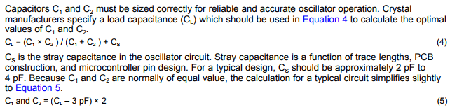
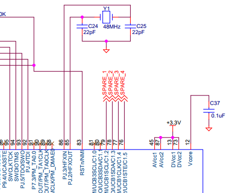
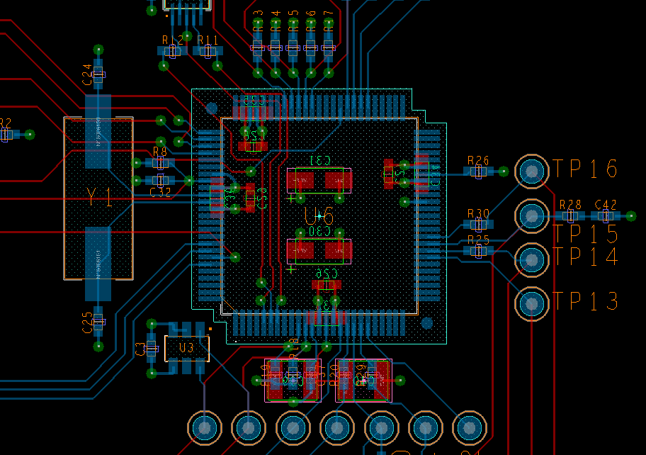
The crystal on my custom board is an Abracon ABLS-48.000MHZ-B2-T with 22pf caps to ground, connected across pins PJ.2 and PJ.3.
I've also used the debugger to check the register value of the CS clock dividers and all the dividers are set to zero, so the HFXTCLK shouldn't be divided before sourcing MCLK.
Not sure what the next thing to look at should be.
Thanks for any help!
Here's the example code that I've been using:
#include "ti/devices/msp432p4xx/inc/msp.h"
#include "stdint.h"

void error(void);

int main(void)
{
    volatile uint32_t i;
    uint32_t currentPowerState;

    WDT_A->CTL = WDT_A_CTL_PW |             // Stop WDT
                 WDT_A_CTL_HOLD;

    P1->DIR |= BIT0;

    /* NOTE: This example assumes the default power state is AM0_LDO.
     * Refer to  msp432p401x_pcm_0x code examples for more complete PCM operations
     * to exercise various power state transitions between active modes.
     */

    /* Step 1: Transition to VCORE Level 1: AM0_LDO --> AM1_LDO */

    /* Get current power state, if it's not AM0_LDO, error out */
    currentPowerState = PCM->CTL0 & PCM_CTL0_CPM_MASK;
    if (currentPowerState != PCM_CTL0_CPM_0)
        error();

    while ((PCM->CTL1 & PCM_CTL1_PMR_BUSY));
    PCM->CTL0 = PCM_CTL0_KEY_VAL | PCM_CTL0_AMR_1;
    while ((PCM->CTL1 & PCM_CTL1_PMR_BUSY));
    if (PCM->IFG & PCM_IFG_AM_INVALID_TR_IFG)
        error();                            // Error if transition was not successful
    if ((PCM->CTL0 & PCM_CTL0_CPM_MASK) != PCM_CTL0_CPM_1)
        error();                            // Error if device is not in AM1_LDO mode

    /* Step 2: Configure Flash wait-state to 1 for both banks 0 & 1 */
    FLCTL->BANK0_RDCTL = (FLCTL->BANK0_RDCTL & ~(FLCTL_BANK0_RDCTL_WAIT_MASK)) |
            FLCTL_BANK0_RDCTL_WAIT_1;
    FLCTL->BANK1_RDCTL = (FLCTL->BANK0_RDCTL & ~(FLCTL_BANK1_RDCTL_WAIT_MASK)) |
            FLCTL_BANK1_RDCTL_WAIT_1 ;

    /* Step 3: Configure HFXT to use 48MHz crystal, source to MCLK & HSMCLK*/


    PJ->SEL0 |= BIT2 | BIT3;                // Configure PJ.2/3 for HFXT function
    PJ->SEL1 &= ~(BIT2 | BIT3);

    CS->KEY = CS_KEY_VAL ;                  // Unlock CS module for register access
    CS->CTL2 |= CS_CTL2_HFXT_EN | CS_CTL2_HFXTFREQ_6 | CS_CTL2_HFXTDRIVE;
    while(CS->IFG & CS_IFG_HFXTIFG)
        CS->CLRIFG |= CS_CLRIFG_CLR_HFXTIFG;

    /* Select MCLK & HSMCLK = HFXT, no divider */
    CS->CTL1 = CS->CTL1 & ~(CS_CTL1_SELM_MASK | CS_CTL1_DIVM_MASK | CS_CTL1_SELS_MASK | CS_CTL1_DIVHS_MASK) |
            CS_CTL1_SELM__HFXTCLK | CS_CTL1_SELS__HFXTCLK;

    CS->KEY = 0;                            // Lock CS module from unintended accesses

    /* Step 4: Output MCLK to port pin to demonstrate 48MHz operation */
    P4->DIR |= BIT3 | BIT4;
    P4->SEL0 |=BIT3 | BIT4;                 // Output MCLK
    P4->SEL1 &= ~(BIT3 | BIT4);

    while (1)                               // continuous loop
    {
        P1->OUT ^= BIT0;                    // Blink P1.0 LED
        for (i = 200000; i > 0; i--);       // Delay
    }
}

void error(void)
{
    volatile uint32_t i;

    while (1)
    {
        P1->OUT ^= BIT0;
        for(i = 20000; i> 0; i--);          // Blink LED forever
    }
}