Part Number: MSP430FR5739
I am trying to determine why I am seeing greater than expected latency when polling a GPIO input and setting a GPIO output during a polling loop. ( NOTE: I realize polling an input in this manner is generally a no-no; but for sake of this discussion, take the code below as-is ) For the record, I can't find a definitive measure of how long it takes to read a pin and then set a GPIO based on the status of that pin. Anyway...
Clock system is setup to accept a 16MHz from a TCXO on XIN.
P2.3 is attached to a signal generator, 10Hz @10% duty cycle.
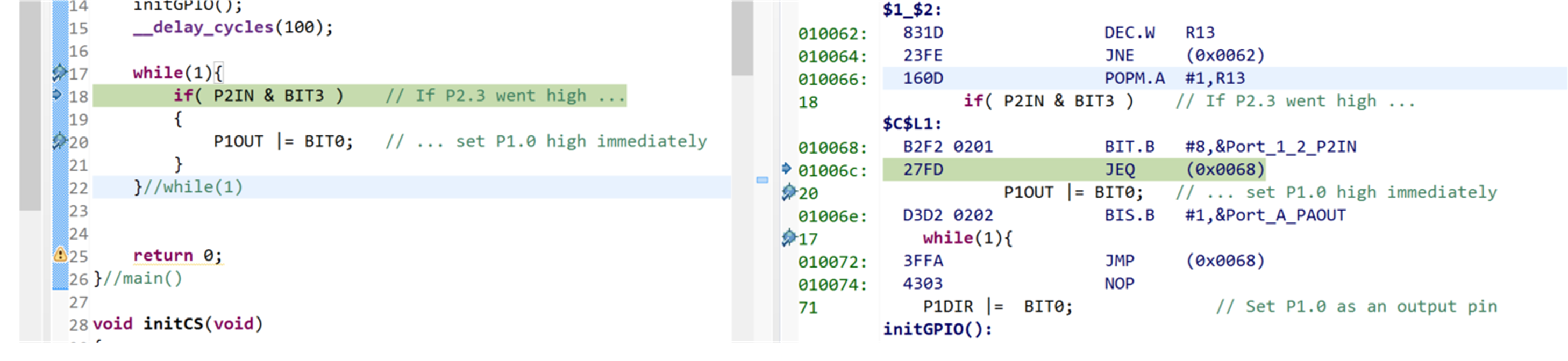
P2.3 is setup as an input with pulldown resistor enabled. Pin 1.0 is setup as an output. Between when P2.3 goes high ( button push ) and P1.0 I am seeing a latency of 620ns. Since my MCLK period is 62.5ns it takes about 9 MCLK cycles to read the pin and set P1.0. This seems excessive to me and I cannot figure out if what I am seeing is the expected behavior.
#include <msp430fr5739.h>

// Prototypes
void initCS(void);
void initGPIO(void);


int main(void)
{
	WDTCTL = WDTPW | WDTHOLD;	// stop watchdog timer

	initCS();
    initGPIO();
    __delay_cycles(100);

    while(1){
        if( P2IN & BIT3 )    // If P2.3 went high ...
        {
            P1OUT |= BIT0;   // ... set P1.0 high immediately
        }
    }//while(1)


	return 0;
}//main()

void initCS(void)
{
       PJSEL0 |= BIT4;                                       // Set PJ.4 as XIN, digital square wave input
       PJSEL1 &= ~BIT4;

       CSCTL0_H = 0xA5;                                       // Unlock password for updating CS

       //CSCTL1 |=                                            // Don't care about this register, not using DCO
       CSCTL2 = SELM__XT1CLK + SELS__XT1CLK + SELA__XT1CLK;   // MCLK source = XT1CLK;  SMCLK source = XT1CLK;
                                                              // ACLK source = XT1CLK
       CSCTL3 = DIVM__1 + DIVS__2 + DIVA__32;                 // MCLK/1;  SMCLK/2;  ACLK/32

       CSCTL4 |= XT1BYPASS | XTS | XT2OFF;                    // Select Bypass mode operation
                                                              // for XT1; select high-freq. mode;
                                                              // Don't need XT2 so turn it off
       do
       {
           CSCTL5 &= ~XT1OFFG;                               // Clear XT1 fault flag
           SFRIFG1 &= ~OFIFG;
           __delay_cycles(10000);                            // Wait around a little while before next check
       } while (SFRIFG1&OFIFG);                              // Test oscillator fault flag


       PJDIR  |= BIT5;      // Set PJ.5 as a GPIO output ( don't need XOUT )

       PJDIR  |=  BIT0;     // Set PJ.0 as SMCLK output
       PJSEL0 |=  BIT0;
       PJSEL1 &= ~BIT0;

       PJDIR  |=  BIT1;     // Set PJ.1 as MCLK output
       PJSEL0 |=  BIT1;
       PJSEL1 &= ~BIT1;

       PJDIR  |=  BIT2;     // Set PJ.2 as ACLK output
       PJSEL0 |=  BIT2;
       PJSEL1 &= ~BIT2;
}//initCS()

void initGPIO(void)
{
    // Pulse output pin P1.0
    P1DIR |=  BIT0;              // Set P1.0 as an output pin
    P1OUT &= ~BIT0;              // Initialize P1.0 to low

    // Sync sensing pin P2.3
    P2DIR &=  ~BIT3;             // Set P2.3 as an input pin
    P2REN |=  BIT3;              // Enable pu or pd on this pin
    P2OUT &= ~BIT3;              // Select pull-down resistor on this pin
    __delay_cycles(5);           // Give time for pullup to settle
}

(1) Do compiler settings ( DEBUG vs. RELEASE mode ) have anything to do with this latency?
(2) Is there a way to lower this latency?
(3) For the record, using an interrupt to set P1.0 results in even greater latency between P2.3 going high and P1.0 going high.