This thread has been locked.

If you have a related question, please click the "Ask a related question" button in the top right corner. The newly created question will be automatically linked to this question.

CCS/MSP430FR4133: ADC counts issues

Part Number: MSP430FR4133

Tool/software: Code Composer Studio

Hi all, 

So bottom line, I'm incredibly confused. I've been stumped by the same issue for a week now and need some help. I am using the MSP430fr4133 and attempting to read from any of the external ADC pins. I have some previous experience with some other microcontrollers so I'm not completely new to this. I have some key questions. As far as hardware, I have attempted reading pins with a constant voltage source, or directly tied to ground and instead and I am reading some count number that is completely independent, however, not independent of temperature, if you were interested. 

1. The sampling and holding time affects the read counts, one above 32 clock cycles, the fluctuations reduce from plus/minus 20 to plus/minus 2. 

2. Changing the reference voltage has no effect on this floating number. 

3. Changing between 8-10-12 bit conversions has no effect on the floating number. 

4. Confirm that when ADCSHP is set to 0, ADCSC starts conversions. If I set it to 0, then the entire conversion doesn't work. I have no timers setup so it wouldn't make sense with it being set to 1, however, it only conducts conversions when the ADCSHP is 1. 

#include <msp430.h>
#include <string.h>
#include <stdio.h>
#include <driverlib.h

void SYSTEMinit();
void UARTinit();
void ADCinit();
int writeUART(char* sentence);
int analog (int channel);
int tempConvert(int counts);

int main(void)
{
char buffer[30];
SYSTEMinit();
UARTinit();
ADCinit();

int temp = 0;
while(1)
{
sprintf(buffer, "ADC 6 %d \n\r", analog(6);
writeUART(buffer);
_delay_cycles(4000000);
}
}

void SYSTEMinit()
{
WDTCTL = WDTPW | WDTHOLD; // Stop watchdog timer

// Configure GPIO
//Init_GPIO();
PM5CTL0 &= ~LOCKLPM5; // Disable the GPIO power-on default high-impedance mode
// to activate 1previously configured port settings
//__bis_SR_register(SCG0); // disable FLL
CSCTL3 |= SELREF__REFOCLK; // Set REFO as FLL reference source
CSCTL0 = 0; // clear DCO and MOD registers
CSCTL1 &= ~(DCORSEL_7); // Clear DCO frequency select bits first
CSCTL1 |= DCORSEL_3; // Set DCO = 8MHz
CSCTL2 = FLLD_0 + 243; // DCODIV = 8MHz
CSCTL4 = SELMS__DCOCLKDIV | SELA__REFOCLK; // set default REFO(~32kHz) as ACLK source, ACLK = 32768Hz
// default DCODIV as MCLK and SMCLK source
}
void UARTinit()
{
//STEP 1 Set UCSWRST Bit
UCA0CTLW0 |= UCSWRST; //Allows UART to be configured
//STEP 2 Initialize all relevant Registers
UCA0CTLW0 |= UCSSEL__SMCLK; //Choses SMCLK as clock source for UART
UCA0BR0 = 52; // 8000000/16/9600 CORRECT 9600 BAUD RATE
//UCA0BR1 = 0x00;
UCA0MCTLW = 0x4900 | UCOS16 | UCBRF_1;
//STEP 3 Configure Ports
P1SEL0 |= BIT0 + BIT1; // set 2-UART pin as Primary non I/O function
//STEP 4 SEt UCSWRST Bit
UCA0CTLW0 &= ~UCSWRST; // Initialize eUSCI
//STEP 5 ENABLE INTERUPTS
__enable_interrupt( );
UCA0IE |= UCRXIE; // Enable USCI_A0 RX interrupt

_delay_cycles(4000000);
writeUART("start");
}
void ADCinit()
{
ADCCTL0 |= ADCSHT_3 + ADCON; // ADCON, S&H=32 ADC clks
ADCMCTL0 &=~ ADCCONSEQ0 + ADCCONSEQ1; //Sets single conversion single channel mode
ADCMCTL0 |= ADCSREF0; //Sets top of scale to VREF and bottom to ground
//ADCCTL1 |= ADCSHP;
ADCCTL1 &=~ ADCSSEL0 + ADCSSEL1; // ADCCLK = MODOSC; sampling timer
ADCCTL1 &=~ ADCSHP; //Initialized ADC conversation after ADCS bit not a timer
ADCCTL2 |= ADCRES_1; //0 gives 8 bit, 1 gives 10 bit, 2 gives 12 bit.
SYSCFG2 |= ADCPCTL6; //Enables ADC inputs. This is critical for all external ports. Temp sensor cannot be configured
//P1SEL0 |= BIT3;

//DECLARE INPUT PINS WHEN WE HAVE THEM. Temp sensor doesnt need to be declared
PMMCTL0_H = PMMPW_H; // Unlock the PMM registers. REQUIRED FOR TEMPERATURE SENSOR
PMMCTL2 |= TSENSOREN + INTREFEN; // Enable internal reference
__delay_cycles(400); // Delay for reference settling

ADCCTL0 |= ADCENC; //Enables ADC. Main bits above can no longer be edited
}
int analog (int channel) 
{
if (channel == 2)
{
ADCMCTL0 = 0x02;
}
if (channel == 3)
{
ADCMCTL0 = 0x03;
}
if (channel == 4)
{
ADCMCTL0 = 0x04;
}
if (channel == 5)
{
ADCMCTL0 = 0x05;
}
if (channel == 6)
{
ADCMCTL0 = 0x06;
}
if (channel == 7)
{
ADCMCTL0 = 0x07;
}
if (channel == 12)
{
ADCMCTL0 = ADCINCH_12;
}
ADCCTL0 |= ADCSC; // starts ADC conversion
while(ADCCTL1 & ADCBUSY);
return ADCMEM0;
}

int writeUART(char* sentence)
{
int i;
for (i = 0; i < strlen(sentence); i++) {
while(!(UCA0IFG&UCTXIFG));
UCA0TXBUF = sentence[i];
}
return i;
}

Any help would be greatly appreciated. Thank you for your time.

Austin

  • Additional information. I compiled the same shortly after writing this post and it broke. If you are completely lost when trying to help resolve this let me know and I will do my best to help.
  • Hi Austin,

    Thanks for taking a look at the ADC peripheral on the MSP430F4133. A few things to look at in your posted code:

    1. In your analog(channel) function, you write ADCMCTL0 wholistically, and not just the channel selection bits. This means you are overwritting your reference selection to 0b000 (VR+ = AVCC and VR– = AVSS). I assume that you only want to change the channel in this function, but maybe it was your intent to change the reference as well.

    2. In your ADCinit() function, you clear ADCCONSEQ0 + ADCCONSEQ1 in ADCMCTL0, but these bits are actually in ADCCTL1. Ultimately, the change to ADCMCTL0 doesn't matter because you overwrite this register in analog().

    3. The MSP430FR4133 has a 10-bit ADC, so there is no 12-bit setting as you mention in your comments.

    4. You determine that the value is valid in ADCMEM0 based on ADCBUSY. I would not recommend this from a timing point of view. Per the User's Guide, the indication that the result register ADCMEM0 has been written is the setting of ADCIFG0. I would recommend that you clear ADCIFG0 in the ADCIFG register, start the conversion, and wait for ADCIFG0 to be set before reading the result. I'll need to check the ADC sequencing again, but I am concerned that it is not a good practice to test only ADCBUSY because the ADCBUSY bit may not be set by the time the CPU fetches the value on the next instruction. There may even be an ADC wakeup period where the ADC clock needs to come active, and the ADC is not actually busy until this happens. I am speculating a bit at the moment as to whether this is your issue, but regardless I would strongly encourage you to test the ADCIFG0 flag instead.

    Regards,
    Walter
  • Walter,

    Thank you for your advice. I have implemented all of your recommendations, however, I am still struggling to read appropriate data. I am now reading and printing the data from two external pins that have been coded in the analog function and declared within the SYSCFG2 register. One is grounded while the other is not connected, despite this, both are reading 705 counts. 

    In analog, all wholistic replacements have been written in the form of ADCMCTL0 = ADCINCH_7;. I have corrected the register to which ADCCONSEQ0&1 are set.

    I am now polling the flag to see if the conversion has completed, per your recommendation. The end of the analog function is below. 

    if (channel == 12)
    {
    ADCMCTL0 = ADCINCH_12;
    }
    ADCIFG &=~ ADCIFG0;
    ADCCTL0 |= ADCENC + ADCSC; 
    while(ADCIFG0 == 0)
    {
    writeUART("CONVERTING");
    __delay_cycles(4);
    }
    return ADCMEM0;

    As I'm sure you are aware, when ADCIFG0  = 0, there is no result pending. Therefore it should print converting at least three as the 8 bit mode takes 10 cycles, and the 10 bit mode takes 12, according to the family guide. However, CONVERTING is not printed at all, and when I tested the code I changed the while statement to (ADIFG0 == 1), at which point it printed CONVERTING indefinitely, implying that the flag is always tripped. Am I able to reset the flag as I did above? The data sheet says it can be reset through software, and I assume this is what it meant. I also tried ADCIFG = 0x00; with no luck. I also tried adding a delay in front of the polling loop and that did not help. 

    I have two questions about the issue. 1) do you think the issue is timing related?  If so, I don't understand the purpose of the sample and holding time, especially if what I am trying to read is steady. The clock choice has been adapted to the SMCLK, which is 8hz. I assume a higher frequency leads to faster calculations and conversions. Is this clock speed to fast given that I am not dividing it at all despite the two opportunities to. Is there a tradeoff?

    2) Would a timing issue give completely wrong information such as 705 counts when the pin is connected to the VSS/GND pin? I would imagine that would mostly inability to read fluctuations or noise overpowering the signal. 

    EDIT: I think I may have found an error. While I have set specific ports in SYSCFG2, I did not select analog function in the P1SEL0 and P1SEL1 registers. When attempting to set 5,6 to their tertiary purpose of A5 and A6, I received the following error.  #20 identifier "PASEL1_L" is undefined main.c in reference to P1SEL1 |= BIT5 + BIT6;. The same line of code for P1SEL0 works just fine. 

    I greatly appreciate your time on this. 

    Austin

  • Hi Austin,

    Austin Ogle said:
    EDIT: I think I may have found an error. While I have set specific ports in SYSCFG2, I did not select analog function in the P1SEL0 and P1SEL1 registers. When attempting to set 5,6 to their tertiary purpose of A5 and A6, I received the following error.  #20 identifier "PASEL1_L" is undefined main.c in reference to P1SEL1 |= BIT5 + BIT6;. The same line of code for P1SEL0 works just fine. 

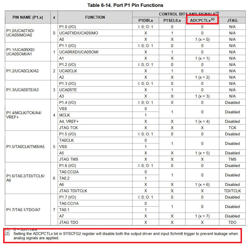
    The MSP430FR4133 does not have PxSEL1 registers; this is why you are getting the error.  Some devices have this register, but not all of them.  The MSP430FR4133 only has PxSEL0.  You only need to select ADCPCTLx.  Below is the documentation on this topic.

    Austin Ogle said:
    As I'm sure you are aware, when ADCIFG0  = 0, there is no result pending. Therefore it should print converting at least three as the 8 bit mode takes 10 cycles, and the 10 bit mode takes 12, according to the family guide. However, CONVERTING is not printed at all, and when I tested the code I changed the while statement to (ADIFG0 == 1), at which point it printed CONVERTING indefinitely, implying that the flag is always tripped. Am I able to reset the flag as I did above? The data sheet says it can be reset through software, and I assume this is what it meant. I also tried ADCIFG = 0x00; with no luck. I also tried adding a delay in front of the polling loop and that did not help.

    ADCIFG0 is a bit mask definition; it is not an actual register value.

    #define ADCIFG0                (0x0001)       /* ADC Interrupt Flag */

    It will always be equal to 1.  This is why when you test ==0 it never runs, and when you test ==1 it always runs.  You want to test the ADCIFG0 bit in the ADCIFG register itself.

    Here is the most basic ADC example I came up with.  I have verified this on hardware.  Can you attempt to run this and confirm ADC operation on your hardware?

    #include <stdint.h>
    #include <msp430.h> 
    
    uint16_t result;
    
    void main(void)
    {
        WDTCTL = WDTPW | WDTHOLD;
    
        SYSCFG2 |= ADCPCTL6;
        PM5CTL0 &= ~LOCKLPM5;
    	
        ADCCTL0 |= ADCSHT_2 | ADCON;
        ADCCTL1 |= ADCSHP;
        ADCCTL2 |= ADCRES;
        ADCMCTL0 |= ADCINCH_6;
    
        while (1)
        {
            ADCIFG &= ~ADCIFG0;
            ADCCTL0 |= ADCENC | ADCSC;
            while ((ADCIFG & ADCIFG0) == 0);
            result = ADCMEM0;
            __no_operation();
            __delay_cycles(1000000);
        }
    }

    Austin Ogle said:
    I have two questions about the issue. 1) do you think the issue is timing related?  If so, I don't understand the purpose of the sample and holding time, especially if what I am trying to read is steady. The clock choice has been adapted to the SMCLK, which is 8hz. I assume a higher frequency leads to faster calculations and conversions. Is this clock speed to fast given that I am not dividing it at all despite the two opportunities to. Is there a tradeoff?

    8 MHz is a bit fast for this ADC.  You want to run it closer to 5 MHz.  The example I posted above uses the MODOSC as the ADC clock source, with a frequency of 5 MHz typical.  The sample and hold time is still needed to charge the sample and hold capacitor.  The sample and hold capacitor is used in the conversion process.

    Regards,

    Walter

  • Thank you Walter! ADC works exactly as intended.

**Attention** This is a public forum