This thread has been locked.

If you have a related question, please click the "Ask a related question" button in the top right corner. The newly created question will be automatically linked to this question.

MSP430FR5969: Setting PxDIR for secondary GPIO functions.

Part Number: MSP430FR5969
Other Parts Discussed in Thread: MSP430FR6989

Hi, 

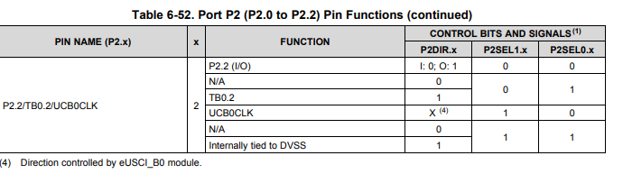
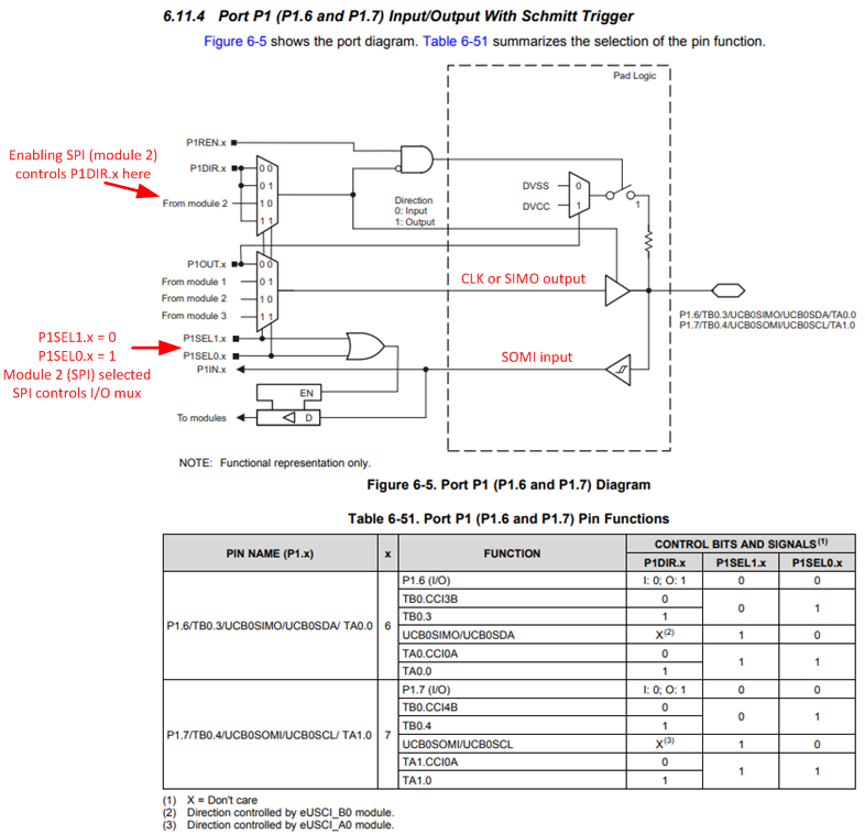
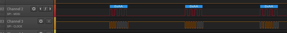
I am using the eUSCI_B as a master SPI and I think I am missing something because I cannot see a clock signal. I did not set the PxDIR register as the manual made it seem like the value of that register was tranferred over for control by the eUSCI module? Anyways I am going back and reading the datasheet more closely and noticing that for P1.7 on the MSP430FR5969 P1.7 is SOMI (MISO) for SPI_B0, but the manual says that the PxDIR direction is controlled by eUSCI_A0 which actually makes no sense to me. Why would a eUSCI_B pin be controlled by a specific instance of eUSCI_A? Do I need to initialize eUSCI_A0 in order to get the clock going? Here's a screenshot for reference:

  • Hi Jennifer,

    That appears to be "typo" and should be (2).  I will work with the product engineer to get that updated.

    Regarding setting up the port pins to use the SPI you need to set the PnSEL1.x and PnSEL0.x bits accordingly for the UCB0SOMI, UCB0SIMO, USB0CLK.

    Specifically, to enable the SPI CLK to appear on the IO pin, you need to set P2SEL1.2 = 1, P2SEL0.2 = 0 as shown in the table.

  • Dennis,
    Do I also need to set the PxDIR register? I now have the clock working after I saw one of your examples ( eusci_b_spi_ex_1_master.c) setting every single pin to an input as well as setting PxSEL0 and PxSEL1. I cannot see any justification for doing that either in the family datasheet or the device specific datasheet. Can you point me to somewhere in the datasheet where it says that this is necessary to do before using the module? Do you need to set the PxDIR register no matter what the function selection is? I was under the impression from datasheets that the PxDIR was strictly for digital I/O.

    Thanks for the help.
  • Here is the code I am referencing: I'm not sure why some of these things are set to inputs, especially if this is supposed to be a *master* example......?


    /*
    * Select Port 2
    * Set Pin 2 to input Secondary Module Function, (UCB0CLK).
    */
    GPIO_setAsPeripheralModuleFunctionInputPin(
    GPIO_PORT_P2,
    GPIO_PIN2,
    GPIO_SECONDARY_MODULE_FUNCTION
    );

    /*
    * Select Port 1
    * Set Pin 6, 7 to input Secondary Module Function, (UCB0TXD/UCB0SIMO, UCB0RXD/UCB0SOMI).
    */
    GPIO_setAsPeripheralModuleFunctionInputPin(
    GPIO_PORT_P1,
    GPIO_PIN6 + GPIO_PIN7,
    GPIO_SECONDARY_MODULE_FUNCTION
    );
  • Hi Jennifer,

    Good question.  The user's guide says to look at the datasheet, specifically at the input/output diagrams, but if you refer to the table you posted earlier you will see the 'X' or don't care in the PDIR control register for those pins tells you don't need to set the PDIR for the SPI function to work.

    The best "official" description is in the family user's guide for this device.

    See section 12.2.5.  Here is a snippet:

    Ultimately, refer to the specific device's datasheet (which is the table you posted).  The table will tell you which pins need their PDIR set to operate for each peripheral that shares that pin.

    The example code above is correct.  It is the comment that is mis-leading "Set Pin 2 to input Secondary Module Function, (UCB0CLK)."  It is not setting this pin as an input, rather it probably should say "Select Pin 2 as  Secondary Module Function, (UCB0CLK)." in my opinion.

    Does this clarify this for you?

  • Hi Dennis,

    I need a ask a few more questions to clarify, if that is alright.

    1. In the part you highlighted it says to look in the device-specific datasheet but the device-specific datasheet has the input-output table that specifies that the PxDIR direction for SIMO, SOMI and SCK is 'X' which it later defines to be 'don't care.' *BUT* the example code would indicate that the PxDIR is the ~opposite~ of a don't-care bit, and my experience with having the clock work when I set PxDIR to input and not work when I don't would indicate that we do in fact *care* about the direction of this pin and that it is the user's responsibility to set it??

    2. I scoured datasheets to find the answer to this question, but was just bounced back and forth between documents: The footnotes on the 'X-don't care' in the eUSCI_B0 PxDIR table slot for all eUSCI_B0 SPI GPIO indicate that:
    "eUSCI_B0 controls the direction of the pin"
    I took this to mean that the module eUSCI_B0 takes care of handling the pin once I set it to secondary-function mode? OR does this actually mean that I should set the PxDIR register *based on how I am using the pin within eUSCI_B0* ?

    3. It is *not* only the comment in the code that is misleading, I am actually having a much bigger problem. If you notice the function is called ~~set to secondary function INPUT~~ . And if you go into the source code of this function it is in fact setting PxSEL0 and PxSEL1 to its secondary function *as well as* setting the PxDIR register to '0,' which is setting the same I/O pin that we just as secondary function to a secondary function INPUT. Why is the example code setting PxDIR at all? I don't see any reason for this in any of the datasheets.

    Since you said that the example code above is correct can you please answer these questions as well?......

    4. Why is the example code setting the *master clock* as an INPUT? My clock signal does not work unless I use the snippet of aforementioned code.

    5. Kind of related to question above: Why is Master-**OUT**-Slave-IN (SIMO) set as an INPUT??? It is most definitely an output, so why does it only work when I set the PxDIR direction to '0' with the example code?

    I also want to say that I find the device-specific datasheet sending me to the family-device datasheet , and the other way around, so I feel like I am going in circles. Can you please refer me to the specific parts of both that answer my questions?

    Apologies for the winded post, but it would really help me out if I could not only understand *HOW* but *WHY* the drivers I am writing/benchmarking work.

    Thank you very much for the help !!
  • Hi Jennifer,

    I think what is causing the most confusion here is the example code.  For now, ignore it.  Let's focus on answering your most pressing question, that is, do you need to set the direction of the GPIO to use these pins for SPI? - Answer is No.

    Why?  As described in the datasheet table with the 'X', these mean exactly that - you don't need to set the PDIR register for the SPI.

    To visualize this, lets look at the pin diagram for P1.6 and P1.7 as an example.  I annotated it to make it more clear how the PIN logic works.  Note, this is straight out of the MSP430FR5969 datasheet.

    Ok, now lets look at the code that makes this possible.  I'm not going to comment on the example code because it is misleading.  Rather I'm posting the code I used on an MSP430FR6989 Launchpad to demonstrate this functionality.  Code is below.  There is a section in the beginning in between a '#if 0 ...endif' that does not get compiled by default.  The code stays in a loop writing '0xAA' as you can see in the logic probe capture.  To see what effect the PDIR register has on the SPI pins, you can make the '#if 0' to '#if 1' and configure the PDIR bits as inputs and try the code again.  You will see the SPI continues to work.  Set the PDIR bits as outputs and try again and you will see SPI continues to work.


    And now for the code:

    /*
    * Example code showing how to initialize UCA0 SPI functionality on shared GPIO pins.
    * MSP430FR6989 launch pad
    */
    #include <msp430.h>
    #define SOMI BIT1
    #define SIMO BIT0
    #define CLK BIT2


    int main(void)
    {

    WDTCTL = WDTPW | WDTHOLD; // Stop watchdog timer

    #if 0
    /*
    * To enable this code stub, set = #if 1
    * Experiment - Set SPI GPIO pins as inputs or outputs and see if it affects SPI - It doesn't!!
    */
    P2OUT = 0;

    P2DIR |= (SOMI | SIMO | CLK); // Set the direction to output
    // or
    //P2DIR &= (SOMI | SIMO | CLK); // Set the direction to input
    #endif

    /*
    * Select the secondary functions on these GPIO pins so they can be controlled by UCA0 SPI
    */
    P2SEL0 |= (SOMI | SIMO | CLK); // Set these bits
    P2SEL1 &= ~(SOMI | SIMO | CLK); // Clear these bits

    PM5CTL0 &= ~LOCKLPM5; //Disable the GPIO power-on default high-impedance mode to activate previously configured port settings

    /*
    * Configure the UCA0 peripheral as a master SPI
    */
    UCA0CTLW0 = UCSWRST; // **Put state machine in reset**
    UCA0CTLW0 |= UCMST | UCSYNC |UCCKPL | UCMSB; // MASTER|Synchronous mode|inactive state-high|MSB first
    UCA0CTLW0 &= ~UCCKPH; // Data changed on first UCLK, captured on following

    UCA0CTLW0 |= UCSSEL__SMCLK; // Use SMCLK as clock source
    UCA0BRW = 0x02; // Set bit rate clock = SMCLK / 2
    UCA0CTLW0 &= ~UCSWRST; // **Initialize USCI state machine - Ready for use**

    _enable_interrupts();

    while(1)
    {
    // Wait for the SPI to be ready
    while(UCA0STATW & UCBUSY);

    // Send a byte
    UCA0TXBUF = 0xAA;

    // Create a small delay so when viewing the MOSI pin there is a gap in the logic probe.
    _delay_cycles(50);

    }
    }

    Jennifer, let me know if you understand and agree that PDIR does not need to be configured to use the SPI.  Modify this code for your device and try it.

    Then we can discuss your other questions.

  • Hi Dennis,
    Thank you for your thorough reply. I am thinking this may have something to do with the fact that I am trying to use SPI in polling mode and not interrupt mode. My code is identical to yours, yet if I do not set the PxDIR register, nothing within the eUSCI_B0 instance for SPI will work. I will not get or send bytes because the clock signal dissapears.
  • Sorry nevermind Dennis you are right. Thank you so much for this detailed help :D

**Attention** This is a public forum