Part Number: MSP430F2274-EP
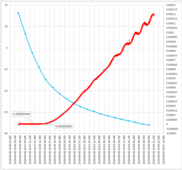
I am working on an msp430f2274-ep where we need to be able to run down at -40 and -50C. When testing the 2274 in a chamber on a small demo board (modified ez430-rf2500 stripped down to only msp430 and a 32.768Khz xtal) we start getting a current ramp around -15C that continues upwards as we cool. See graph below for data point plotting. We are using a keysight B2901 for current measurements and a 34792A DAQ to record temperature right on the outside of the package (K type thermocouple taped to the top of the msp430 with kapton tape)
We tried a board without conformal coat and one with conformal coat, no change in current draw. This happens across the multiple samples we have built up.
What test artifacts (testing, code, results) does TI have to support the LPM3 current draw maximum of 1.5uA down to -55C as stated in the datasheet?
What might we be doing wrong, either with the XTAL or VLO (we have tried both) that is causing this problem?
The code we are using is as follows:
#include "msp430.h"

void configWDT();
void configClocks();
void configGPIO();

static volatile char mode_set;

void main(void)
{                                           //Configuration routines
    configWDT();                            //Watchdog Timer+ Registers
    configGPIO();                           //General purpose pin io registers
    configClocks();                         //Basic Clock Module+ Registers

    mode_set = 0;

    while(1)
    {
        if(mode_set == 0)
            __bis_SR_register(LPM3_bits + GIE);     // Enter Low Power Mode 3 (LPM3) w/interrupt

        else if(mode_set == 1)
            __bis_SR_register(GIE);
    }
}

void configWDT(void)
{
    WDTCTL = WDTPW + WDTHOLD;   // Disable the watchdog timer.
                                // WDTPW        (bits 15 to 8)  = 5Ah.  WDT password.
                                // WDTHOLD      (bit 7)         = 1h.   Disables the WDT.
}


void configClocks()
{
    /* original clock functionality with XTAL and external crystal oscillator */
    //DCOCTL = 0x00;
    //BCSCTL1 = XT2OFF + DIVA_3;
    //BCSCTL2 = SELM_3 + DIVM_3;
    //BCSCTL3 = XCAP_3;

    /* clock functionality with VLO */
    DCOCTL = 0x00;
    BCSCTL1 = XT2OFF + DIVA_3;
    BCSCTL2 = SELM_3 + DIVM_3 + SELS;
    BCSCTL3 = LFXT1S_2 + XCAP_3;
}

void configGPIO(void)       // GPIO Register configuration
{
    //P1
    P1OUT = 0xFF;
    P1DIR = 0x00;
    P1SEL = 0x00;

    P1REN = BIT2;          // P1.2 Enable Pullup/Pulldown
    P1OUT = BIT2;          // P1.2 pullup
    P1IE = BIT2;           // P1.2 interrupt enabled
    P1IES = BIT2;          // P1.2 Hi/lo falling edge
    P1IFG = 0x00;

    //P2
    P2DIR = BIT0;
    P2OUT = 0x00;
    P2SEL = 0xC0;
    P2IE = 0x00;
    P2IES = 0x00;
    P2IFG = 0x00;

    //P3
    P3OUT = 0x00;
    P3DIR = 0xFF;

    //P4
    P4OUT = 0x00;
    P4DIR = 0xFF;
}


// Port 1 interrupt service routine
#pragma vector=PORT1_VECTOR
__interrupt void Port_1(void)
{
    P2OUT ^= BIT0;
    P2IFG &= ~BIT0;
    P1IFG = 0x00;                             // P1.2 IFG cleared

    mode_set = P2OUT;
    __bic_SR_register_on_exit(LPM3_bits);
}