This thread has been locked.

If you have a related question, please click the "Ask a related question" button in the top right corner. The newly created question will be automatically linked to this question.

MSP430F5528: MSP430 crazy current consumption (up to 600mA !)

Part Number: MSP430F5528
Other Parts Discussed in Thread: MSP430F5529

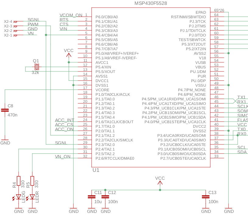
Some time ago I built a prototype (say prototype No 1) of a simple, straight forward, system built around a MSP430F5528 (schematics below), this prototype worked at once and I have so far not found any issues.

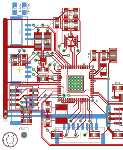
Recently I had to make some changes, mainly on the PCB. I have redrawn the schematics (also provided below) and the board and built a new prototype (say prototype No 2). When I connected this prototype to power it consumed a lot of current (couple of tens milliamps) and this consumption gently built up to hundred, two hundred milliamps even hundreds of milliamps in more or less a minute.

Of course I have checked schematics and PCB over and over but did not find any reason for this issue.

To make sure I have built two additional prototypes No 1, soldering only the MSP430 and nothing else. The consumption is around 1-2 mA in both cases.

I also built two more prototypes No 2 with only the MSP430, and observe the same behavior.

In the mean time my first prototype No 2 seems to be dead i.e. consumes no more power after quite some trials.

Anyone has an idea ?

My MSP430 is in a 64 pin RGC package, I observed that this package has two additional 'contacts' on each side between the first and last 'pin' and the corner. These contacts only appear on the side of the package, not on the bottom. In one place I have a via to ground precisely under these contacts, there is thus  slight chance that on of these contacts may be grounded (also I have not been able to obtain any evidence of such a short) could that explain this issue ?

Prototype No 1

Prototype No 2

Prototype No 2 PCB (part):

  • Based on this schematic snippet no obvious failure can be seen the question is did you aligned the SW according to the different connected GPIOs.
    Proto #2 is not used USB right while hope this is considered in SW as well.
  • Hi Dietmar,

    nothing is connected to any pin as no other component are mounted, so basically this respects TI recommendations for unused pins (left open).
    I didn't even connect the JTAG connector except on the first prototype and CCS reports 'unknown device'.
    Yes, USB is not used anymore; the only issue I can see (but with an unpopulated board this is the same on both prototypes) is that PUR should be pulled-down. I tried, it even increases the consumed current...

    Thanks,
    Marc
  • When unconnected pins are configured as inputs (the default), the floating voltage can partially activate both complementary transistors, and the cross currents will increase power consumptions greatly. Unused pins must be configured as outputs (see table 1-3 in the User's Guide), or as inputs with pull-up/-down.
  • Hi,

    correct all pins requires termination either you configure them output high/low or input with pull up/downs enabled.

    Any floating GPIO (also JTAG pins) contributes to current consumption. And TI does not recommend to leave unused ports open in the users guide following table defines how terminate unused pins:

  • Dietmar,

    this is a critical issue for me, I have many pressure to finish these prototypes ASAP, this is for a extremely important market for my company. I have not yet seen an answer for my initial questions.

    With these devices powered, current raises until hundreds of milliamps in less than a minute or two and they obviously 'burn'. There is no chance to program the device in such short time, I don't believe the state of gpio pins can matter in this case and certainly not contribute to such an important power consumption.

    I have six different prototypes based on the same design, there is no sole component connected, all pins are floating, on the first prototype all three devices consumes a steady 1 to 2mA for minutes on the second all three exhibit totally abnormal power consumption. Obviously something is physically wrong and I kindly request TI attention to solve this issue. I'm ready to provide whatever information you need.

    Yes, I believe that all pins are correctly terminated since this table indicates only Vss and Vcc connections for power pins and most other pins can be left open, which is the case. The only exceptions I can see might be:

    PUR - this pin is indeed left open, I tried on one device to ground it with a 1M resistor, this did not fix the issue, but it might be already too late for these devices,

    RST - at first trial I put the pullup resistor in place, but I suspected external components could be the cause of the issue so I removed everything,

    XT2IN - indeed not connected to VSS as a XTAL is planed.

    Once again, of the first prototype all three I mounted have a normal power consumption even with these pins open.

    I have made some additional tests on my second prototype:

    • I checked all pins to GND and VCC for shorts and couldn't find anything,
    • I cut the power path to all DVCC and AVCC, current falls to 0, so it definitely is the MSP that is consuming the current,
    • Although my ohm-meter measures resistance on higher voltage (5 to 6 Volts) than acceptable for a MSP I measured roughly 130Ohm between VCC and GND on the devices that have this issue; on a correct prototype the current would grow significantly only after applying more than 8 Volts, and not at all in the same proportions.

    Thanks for your help,

    Marc

  • Thanks Clemens, but I think you would agree that:

    - in order to program GPIO pins as output you need to be able to power up the device and program it, when the devices consumes hundreds of milliamps after, say, 30 seconds, you don't have such a chance and it's hard to believe this might be the problem,
    - If you check TI MSP430F5529 launchpad schematics, please note that all these pins are left open, and the device works perfectly well,
    - I have six devices, three of prototype No 1 behave quite normally after power up, three of prototype No 2 don't, whilst on all prototypes these pins are left open.

    I can't see any reasonable explanation other that a physical issue the my PCB. An obvious reason would be for example connecting power reverse. I checked that over and over I definitely can't find any reason such a current, and still found no electrical difference between my two different prototypes.

    Kind regards,
    Marc
  • Retokid,

    you mentioned that you made ABA swap right which means you took a high current part from protoyp No2 to a prototyp No1 board and there no high current appeared correct?
    Did you also tried to take this unit to a socket board program it to LPM4 and measure the current to see if it is damaged.
    This is important to check that the parts are not damaged permanently.

    You also mentioned that your part is not programmed when you solder it correct? In such a case the device would recognize that RST vector is not programmed and put part into LPM4 with all GPIOs set to input floating.

    Are there any voltages above DVCC applied to any GPIO?
    How the supply voltage is generated in both protoypes?

    You said you made changes from protoype 1 to 2 can you list these changes in detail?
  • Hi Dietmar,

    no, I can't remove these parts, once they are soldered they canot be removed (or at least I am not equipped to do that).

    I did mount 6 different prototypes (3x No1 3x No2) with different MSPs. All prototypes No 1 seem to behave normally, all prototypes No 2 consume more and more current, get hot if I let it go up to more than 600mA. I guess at that point they are defect, I did not try to have them programmed because the time to do that I guess they are probably molt down. I never let the power for more than a couple of seconds until yet.

    Yes, I believe what you say is correct. The devices are soldered without being programmed (sorry I did not mention that before), they should indeed go immediately in some kind of LPM state.

    I can't see any voltage applied to any pin except the DVCC and AVCC pins.

    I am using a power supply, the same in all cases, but I agree there could be an issue with this power supply.

    What I plan to do next is make a new prototype No 2 with fresh MSP and the minimal standard components (RST pull-up, PUR pull-down, VCORE capacitor and connect the whole stuff to a logging DVM so that I can send you a voltage/current diagram.

    The only changes I made from schematics point of view is removing the USB components as I am (at this stage) not using USB.
    From PCB point a view I redraw my entire PCB and to facilitate this I reassigned a number of GPIO pin functions, this should have no impact as the pins are not connected to any components so far. If it helps I can send the Eagle schematics and board files.

    Kind regards,
    Marc
  • Hi Marc,

    if you use unprogrammed parts it shoudl not matter if you have GND or 3V to GPIOs. If you're parts gets damaged I only can imagine your supply is connect incorreclty. Looks like polarisation is incorrect. I think tracing DVCC, Vcore, RST and GND with a scope would help here.

    I mean a short on the PCB itself should draw the current on the PCB but not on MSP site. Did you measured the connecton on all supply pads to GND before you solder the part ensuring electrical connections are correct?
  • Hi Dietmar,

    I agree, I believe all GPIO pins canot be part of the issue.

    Yes, I tested all power connections to VCC and GND, of course this seems to be OK. If there was a short anywhere I would observe an immediate and important current, which is not the case.

    I will try to catch all signals at once, but specially will try to measure VCC and current, that will clarify the situation. I expect to do this on thursday, I'll send a new post.

    Can you get any information on the 'extra' contacts that appear on side of the RGC package near the edges ?
  • The easiest way to find a short, i.e., the location where the most current flows, is with a thermal camera (or alcohol, or freeze spray).

    Alternatively, use a sensitive voltmeter to measure the voltage drop along the tracks.

  • Hi Dietmar,

    I have built two additional prototypes in order to measure and log the current, Vcc, Vcore and Reset.

    The peak current did not raise to the same amounts as what I have measured before, although it is still abnormal:

    Below, Vcc (yellow), VCore (pink) and reset (blue), I believe the ripple is due do the current variations (see below).

    This is the current measured over more or less the same period in Amps:

    There are some peaks at more then 60mA, in y previous observations I would see ore or less the same scheme (oscillating but increasing current) but it would grow much quicker.

    As we are in a hurry with the development of the intended device, I decided to abandon the use of the 5528 in VQFN package in favor of a 5529 in PDIP package, I believe these issues are related to the manual soldering. We will try the VQFN package once the rest of the circuit is validated and once we have time to sort out the issue.

    Thanks for trying to help.

  • Hi,

    thanks for the measurements. This really looks like a floating effect but the large spikes are really strange, never seen this before on not programmed part.

    But if you can live with the F5529 in PDIP so far it's good to hear when you furhter investigate the QFN behavior and still see the problem you can open a new thread refering to this one. So far I will close this thread.

  • Hello,

    as I read thru this your posts, I emebered that time I has some similar sounding issues.

    On a MSP430F5529 in VQN case with 80 pins, when connecting USB , I think it was started by connecting the usb, the MSP started to draw a lot of current and getting hot very fast, it was never broken,

    I disconnected it from power after maybe 10 seconds and could reprogram and debug the device, sometimes this would occur and sometimtes not, however back at that time I did not further inverstigate this, since it luckily only happened on one board, so I did blame it on myself maybe bad soldering or something else, but now that I kind of read about it again, I think maybe there is something else to it.

    Adn one additinoal question because someone did write about MSP430F5529 in PDIP package? I couldnt find it, is there really such a thing as F5529 in thru hole?

    Or did you mean something different?

  • Hi seb, thanks for the information. I'm sure that some kind of instability is causing this current, unfortunately I really have no time at this moment do investigate further.

    You are right, my confusion, it's not PDIP, it's PQFP (PLASTIC QUAD FLATPACK), with nice pins to  solder ,-)

    Regards,

    Marc

  • Hi Retokid,
    because you will go with a different package variant and the you think the issue might related to soldering I will close this thread.
    If you need assistance again if the behavior appears during future work pls let us know.
  • Hi Dietmar,

    OK, fine.

    Thanks.

**Attention** This is a public forum