A related question is a question created from another question. When the related question is created, it will be automatically linked to the original question.
If you have a related question, please click the "Ask a related question" button in the top right corner. The newly created question will be automatically linked to this question.
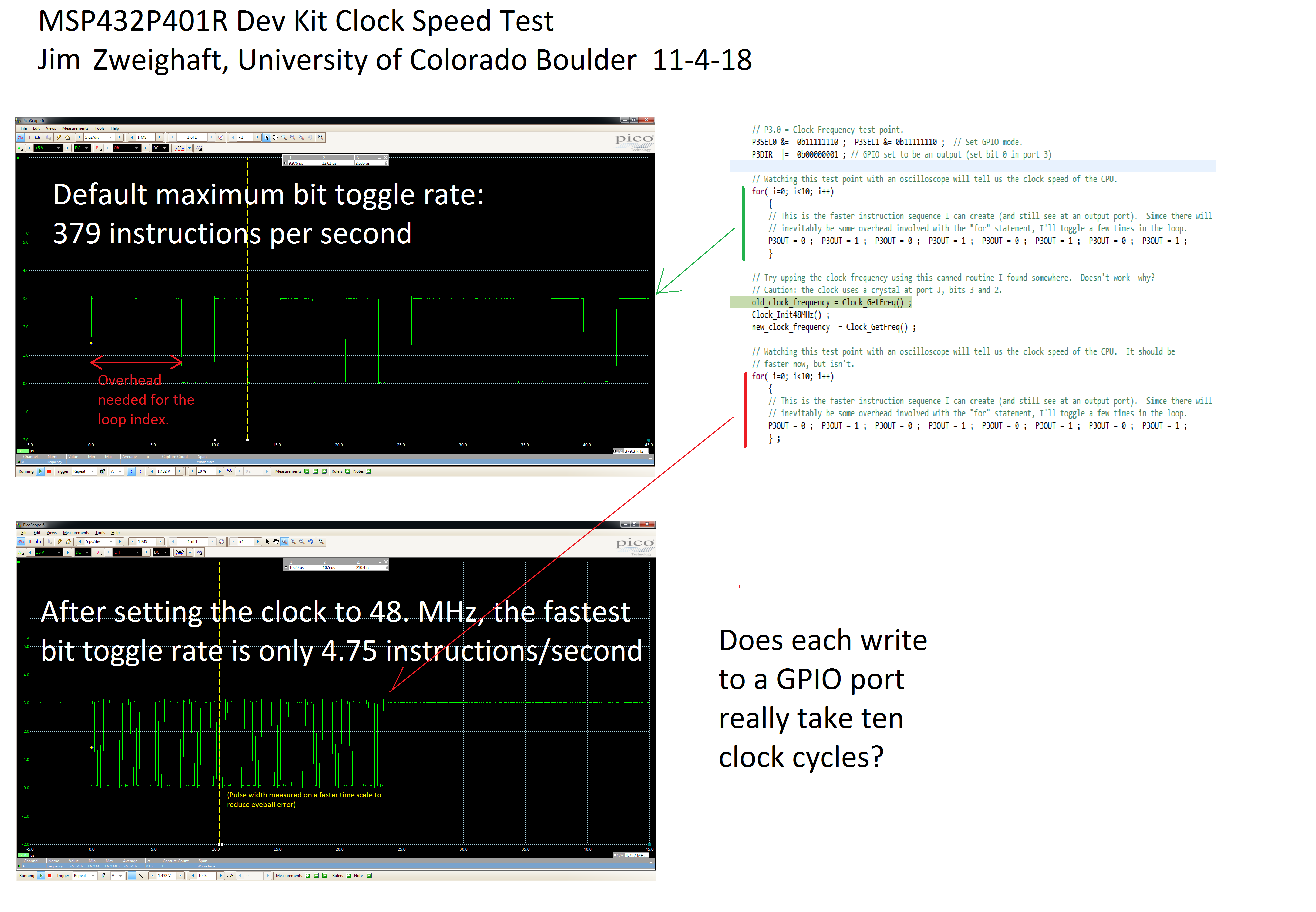
CCS/MSP432P401R: Code execution speed: 10 clocks per instruction? I thought RISC processor ran at 1 clock per instruction.
Hello James,
RISC architectures try to do CPU register based operations in one clock cycle.
IO operations, like GPIO writes, are read-modify-write operations on Cortex M, and take more than one or two cycles. The port peripherals of this controllers are more complex than that of older 8-bit MCUs, and need to take care that all states (output registers and read-back registers) are consistent. Moreover, probably you run your code from FRAM which needs 3 wait states @48 MHz.
To speed up GPIO toggling you should use bitbanging and run a code from RAM.
This fast GPIO toggle is no use case for MCU based on Cortex 4MF. Pulling a GPIO pin up and down in a mega-hertz loop renders the whole MCU peripherals useless.
I deliberately wrote to the entire port to try to avoid a read-modify-write cycle which of course would take longer. This is the simplest thing I could think of that I could verify with an oscilloscope.
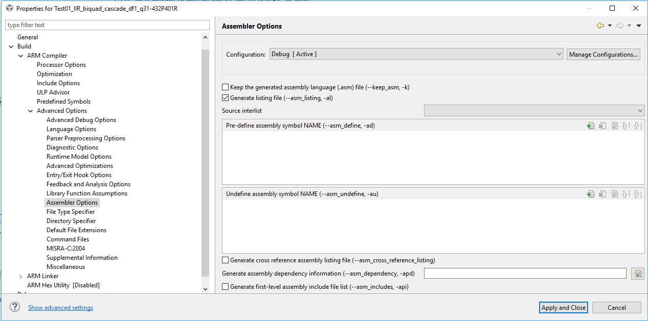
PS- I am not using FRAM, though I understand that's as fast as RAM. I will look into moving this test code from Flash ROM to RAM and see what the difference is. I will also see if I can get CCS to generate a listing file so I can see what's happening at the assembly level. Too bad the wording "listing" does not appear in the CCS User's Guide.
You can use View -> Memory Allocation or the project map file to find how your code and data are allocated.
FRAM works without wait states up to 24 MHz. As I remember, RAM has no wait states up to full speed @48 MHz. I will not confirm RAM speed right now. It is 2:38 a.m. my local time.
James Zweighaft said:
Too bad the wording "listing" does not appear in the CCS User's Guide.
Assembly feature is a compiler feature, not CCS. --asm-listing feature is an old feature on UNIX/Linux world.
The MSP432 is a Flash-based device. It does not use FRAM. Also, the 3 Wait States associated with each Flash access doesn't impact your performance as much as you would think due to the presence of a wide (128b) prefetch buffer. This prefetch means that, for linear code, you only pay the 3WS penalty every ~8 instructions, thereby greatly reducing the performance impact. This mechanism, plus some of the latencies in the system bussing, means that "running from SRAM" doesn't result a meaningful improvement in speed.
As Tomasz referenced, the access to the peripheral registers is slower than for SRAM for CPU registers. According to Table 5-3 (Peripheral Register Access Latency) in the MSP432 datasheet, peripheral (Read or Write) access can take 2-5 cycles, with the actual value dependent on the opcode used in the previous cycle plus the status of the sytem buses during the access (i.e. is the DMA doing something else some other higher-priority activity).
Per some of the comments from Tom, the first thing I would look at is the dissasembled code to see what actual instructions are running and whether any overhead has been inserted. I would also look at the register-level example msp432p401x_cs_03, which shows how to output the MCLK to a pin (P4.3) so that you can verify you are running at 48MHz and eliminate that from your debugging efforts).
Thanks for the insights. I was able to create a listing file and saw that that the GPIO write results in 3 assembly language instructions. Maybe a register-register add can be dome in one clock cycle, but not these instructions. I updated my data with the assembly code on the far right if you care to take a look.
That listing surprises me; I'd have expected the compiler to optimize out the repeated loads of the destination address and the reused constants zero and one, at least within the unrolled loop you wrote.
Which compiler version are you using and what optimization level is specified in the CCS project?
The MSP432 is a Flash-based device. It does not use FRAM.
Flash, of course.
Bob Landers said:
due to the presence of a wide (128b) prefetch buffer. This prefetch means that, for linear code, you only pay the 3WS penalty every ~8 instructions
In my modest opinion, it is true if a prefetch unit has at at least 64 bits wide interface to Flash. Is it true? Does code prefetching exist for SRAM operations?
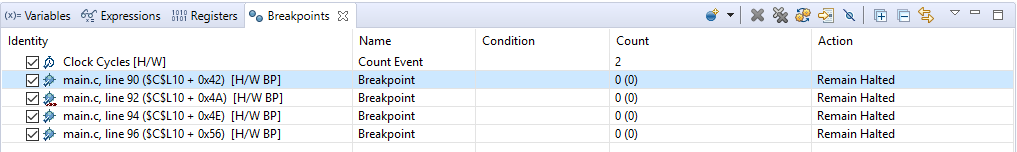
I took an empty driverlib TI example project, than added:
P3OUT = 0; P3OUT = 1; P3OUT = 0;
Debugger Clock Cycles feature shows 13 cycles to execute first and second statement.
James, I don't know about MSP432, but I know other mcu's based on ARM Cortex M, where port I/O is mapped to CPU domain, and port read/write instruction can be executed in 1 CPU cycle. I am using this right now on Cortex-M0+ device with 48 MHz MCLK, with code executed from RAM.
/* --COPYRIGHT--,BSD
 * Copyright (c) 2017, Texas Instruments Incorporated
 * All rights reserved.
 *
 * Redistribution and use in source and binary forms, with or without
 * modification, are permitted provided that the following conditions
 * are met:
 *
 * *  Redistributions of source code must retain the above copyright
 *    notice, this list of conditions and the following disclaimer.
 *
 * *  Redistributions in binary form must reproduce the above copyright
    notice, this list of conditions and the following disclaimer in the
 *    documentation and/or other materials provided with the distribution.
 *
 * *  Neither the name of Texas Instruments Incorporated nor the names of
 *    its contributors may be used to endorse or promote products derived
 *    from this software without specific prior written permission.
 *
 * THIS SOFTWARE IS PROVIDED BY THE COPYRIGHT HOLDERS AND CONTRIBUTORS "AS IS"
 * AND ANY EXPRESS OR IMPLIED WARRANTIES, INCLUDING, BUT NOT LIMITED TO,
 * THE IMPLIED WARRANTIES OF MERCHANTABILITY AND FITNESS FOR A PARTICULAR
 * PURPOSE ARE DISCLAIMED. IN NO EVENT SHALL THE COPYRIGHT OWNER OR
 * CONTRIBUTORS BE LIABLE FOR ANY DIRECT, INDIRECT, INCIDENTAL, SPECIAL,
 * EXEMPLARY, OR CONSEQUENTIAL DAMAGES (INCLUDING, BUT NOT LIMITED TO,
 * PROCUREMENT OF SUBSTITUTE GOODS OR SERVICES; LOSS OF USE, DATA, OR PROFITS;
 * OR BUSINESS INTERRUPTION) HOWEVER CAUSED AND ON ANY THEORY OF LIABILITY,
 * WHETHER IN CONTRACT, STRICT LIABILITY, OR TORT (INCLUDING NEGLIGENCE OR
 * OTHERWISE) ARISING IN ANY WAY OUT OF THE USE OF THIS SOFTWARE,
 * EVEN IF ADVISED OF THE POSSIBILITY OF SUCH DAMAGE.
 * --/COPYRIGHT--*/
/******************************************************************************
 * MSP432 Empty Project
 *
 * Description: An empty project that uses DriverLib. In this project, DriverLib
 * is built from source instead of the usual library.
 *
 *                MSP432P401
 *             ------------------
 *         /|\|                  |
 *          | |                  |
 *          --|RST               |
 *            |                  |
 *            |                  |
 *            |                  |
 *            |                  |
 *            |                  |
 * Author:
*******************************************************************************/
/* DriverLib Includes */
#include <ti/devices/msp432p4xx/driverlib/driverlib.h>
#include <ti/devices/msp432p4xx/inc/msp432p401r_classic.h>

/* Standard Includes */
#include <stdint.h>
#include <stdbool.h>

#include <arm_math.h>
#include <arm_const_structs.h>

int main(void)
{
    /* Stop Watchdog */
    MAP_WDT_A_holdTimer();

    //![Simple CS Config]
    /* Configuring pins for peripheral/crystal usage and LED for output */
    MAP_GPIO_setAsPeripheralModuleFunctionOutputPin(GPIO_PORT_PJ,
    GPIO_PIN3 | GPIO_PIN2, GPIO_PRIMARY_MODULE_FUNCTION);
    MAP_GPIO_setAsOutputPin(GPIO_PORT_P1, GPIO_PIN0);

    /* Just in case the user wants to use the getACLK, getMCLK, etc. functions,
    * let's set the clock frequency in the code.
    */
    CS_setExternalClockSourceFrequency(32000,48000000);

    /* Starting HFXT in non-bypass mode without a timeout. Before we start
    * we have to change VCORE to 1 to support the 48MHz frequency */
    MAP_PCM_setCoreVoltageLevel(PCM_VCORE1);
    MAP_FlashCtl_setWaitState(FLASH_BANK0, 1);
    MAP_FlashCtl_setWaitState(FLASH_BANK1, 1);
    CS_startHFXT(false);

    /* Initializing MCLK to HFXT (effectively 48MHz) */
    MAP_CS_initClockSignal(CS_MCLK, CS_HFXTCLK_SELECT, CS_CLOCK_DIVIDER_1);
    //![Simple CS Config]

    P3OUT = 0x00;
    P3OUT = 0x01;
    P3OUT = 0x00;
    P3OUT = 0x01;
    P3OUT = 0x00;

    P3MAP01 = 0x00;
    P3MAP01 = 0x01;
    P3MAP01 = 0x00;

    /* Configuring SysTick to trigger at 12000000 (MCLK is 48MHz so this will
    * make it toggle every 0.25s) */
    MAP_SysTick_enableModule();
    MAP_SysTick_setPeriod(12000000);
    MAP_Interrupt_enableSleepOnIsrExit();
    MAP_SysTick_enableInterrupt();

    /* Enabling MASTER interrupts */
    MAP_Interrupt_enableMaster();

    while (1)
    {
        MAP_PCM_gotoLPM0();
    }
}

void SysTick_Handler(void)
{
    MAP_GPIO_toggleOutputOnPin(GPIO_PORT_P1, GPIO_PIN0);
}
OK, I see what's going now. The default complier used by CCS (source and model number unknown) considerd it an "optimization" to use 1 instruction instead of 3. When I enabled level 0 I got a single line of assembly for my very simple bit toggle C statement (e.g. P3OUT = 0 ; ) I hadn't considered the effect of te pipeline but hear that's not a major issue in this case anyway.
With Optimizations turned off, here is the assembly code the compiler spits out for a single bit change:
It's not clear to me why I need optimizations turned on to get this efficiency, but then I'm an old assembly language hack myself and don't trust compilers.
-Jimmy Z
PS- I had optimizations turned off becuause I don't require maximum speed and they sometimes confuse the debugger.
I belong to Zilog Z80 generetion.
Being DEC team member, I have learned to trust to out of order execution, speculative optimizations, cache coherency, etc.
Trust and verify.
Wish you luck!