


Hello,
I am currently trying to initialize LFXT to use an external clock signal on LFXIN. I have included the code below, but first I will step through my process:
First we set the PJSEL bits knowing that we are going to use an external oscillator which uses LFXT Bypass:
I then unlcok the CS register space, and set the appropriate configurations for CSCTL1 through CSCTL4. I believe this is where something is going wrong as we want the External Clock, as ACLK will source the UART at 32.768kHz.
1. CSCTL1 is set to DCO 8MHz

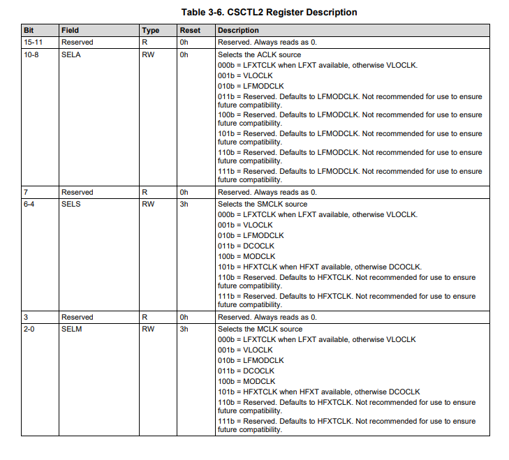
2. CSCTL2 is set to LFXTCLK, DCOCLK and DCOCLK for SELA, SELS and MCLK respectively.
3. CSCTL3 is set to Div 1.

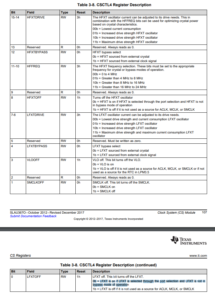
4. CSCTL4 is set to LFXT Bypass and and LFXT Enable (this is where I believe the issue is coming from)

Here is the code for this portion:
static void clock_init(void)
{

        PJSEL1 &= ~0x10;            // pj.4 .. LFXIN EXTERNAL OSCILLATOR mode
	PJSEL0 |=  0x10;            // pj.4 .. DONT CARE

        /*
	    NOTE: With above setting PJ.4 and PJ.5 operate in crystal mode
	*/
	CSCTL0 = 0xA500;            // unlock CS register space
	CSCTL1 = (6 << 1);          // DCO --> 8MHz (trimmed)
	CSCTL2 = (3 << 4) | 3;      // SELA = LFXTCLK, SELS = DCOCLK, MCLK = DCOCLK
	CSCTL3 = 0;                 // ACLK source /1, SMCLK source /1, MCLK source /1
	CSCTL4 &= ~(1 << 0);         // LFXT ENABLE or DISABLE, currently ENABLED
	// selection and LFXT is in bypass mode
	// of operation
	CSCTL4 |= (1 << 4);      // LFXT BYPASS. BYPASS FOR EXT CLK

	/*
	    Wait for external clock signal to stabilize
	    NOTE: this takes a few thousand loops at 1MHz
	*/
	do
	{
		CSCTL5 &= ~LFXTOFFG;
		SFRIFG1 &= ~OFIFG;
	}
	while (SFRIFG1 & OFIFG);
}
Here is also the description of LFXT and its configurations:

The above code appears to execute nominally, and the issue I run into is when I initialize port 4 pins 2 and 3 to use UART (2 is TxD and 3 is RxD). See code below.
The code runs into an issue and crashes once the code that sets P4DIR has been executed, at which the hardware begins consuming 300uA constant current with 20mA spikes at roughly 13Hz. Note that the hardware is not the issue, as I have tested the hardware with a crystal oscillator, and it works great.
	/*
		P4.0 - out .. RF_CS
		P4.1 - out ... ADXL_Power
		P4.2 - out .. TxD - UCA0
		P4.3 - in ... RxD - UCA0
		P4.4 - out .. Don't come out
		P4.5 - out .. Don't come out
		P4.6 - out .. Don't come out
		P4.7 - out .. Don't come out
	*/
	// ....................... 76543210
	P4OUT  = 0x01;			// 00000000
	P4REN  = 0x00;			// 00000000
	P4DIR  = 0xF7;			// 11110111;

#if defined (WIRED_INTERFACE)
	P4SEL0 = 0x00;			// 00000000
#else
	P4SEL0 = 0x0C;			// 00001100
#endif
	P4SEL1 = 0x00;			// 00000000
	P4IES  = 0x00;			// 00000000
All help would be appreciated as I have been stuck on this issue for a few days now. Please let me know if any extra information is needed.
Thanks,
Chris

