Other Parts Discussed in Thread: MSP430WARE, MSP-EM-DESIGN-CENTER
Hello Champs,
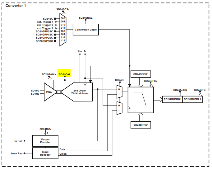
One of my customer is considering to measure current using shunt resistor with MSP430F6736(or F6736A).
At this moment, they got an issue regarding SD24 as below.
<Environment>
- HW using 1phase EVM, SW using SD24 driver library example on the MSP430Ware and modified it.
- Source code : attached
- Symptom : a single channel SD24 conversion result values are grouped with two value range when I repeat to collect the data and reset the MCU again and again.
- Detail explanation :
- A result values averaged with more than 2,000~10,000 samples and saw data three times via break point using JTAG.
- At this point these three data has under 2,000 gap.
- But when I reset in the CCS and run again and saw the data after triggered break point, sometimes it has over 5,000 gap.
For example, First sample average was 67092163, 67090965(1198 gap with first), 67090893(72 gap with 2nd average).
But do the reset and check the second sample average, then 67100153, 67098878(1275 gap), 67099391(-513 gap) showed gap between 1st and 2nd sample over 7000.
- It happens always when the condition SD24 input pins are open, short or some sort of level.
- This case, OSR : 512, GAIN : 16, Opened SD24 input pin.
- More comments
1. When OSR was 512, the data range would be 0 ~ 2^27(-FSR ~ +FSR). The middle(0V) would be 67108864.
2. With my calculation, value gap 4096 for the OSR 512 would be 1bit LSB difference at the 15bit.
3. It is not improved with below actions
- Change Gain, Main and Modulator Frequency, VREF as External 1.2~1.4V(using resistor dividor), SD24 input as open, short, connect shunt.
Would you please guide me if you have any experience regarding this or some idea?
Thank you.
/* --COPYRIGHT--,BSD
 * Copyright (c) 2017, Texas Instruments Incorporated
 * All rights reserved.
 *
 * Redistribution and use in source and binary forms, with or without
 * modification, are permitted provided that the following conditions
 * are met:
 *
 * *  Redistributions of source code must retain the above copyright
 *    notice, this list of conditions and the following disclaimer.
 *
 * *  Redistributions in binary form must reproduce the above copyright
 *    notice, this list of conditions and the following disclaimer in the
 *    documentation and/or other materials provided with the distribution.
 *
 * *  Neither the name of Texas Instruments Incorporated nor the names of
 *    its contributors may be used to endorse or promote products derived
 *    from this software without specific prior written permission.
 *
 * THIS SOFTWARE IS PROVIDED BY THE COPYRIGHT HOLDERS AND CONTRIBUTORS "AS IS"
 * AND ANY EXPRESS OR IMPLIED WARRANTIES, INCLUDING, BUT NOT LIMITED TO,
 * THE IMPLIED WARRANTIES OF MERCHANTABILITY AND FITNESS FOR A PARTICULAR
 * PURPOSE ARE DISCLAIMED. IN NO EVENT SHALL THE COPYRIGHT OWNER OR
 * CONTRIBUTORS BE LIABLE FOR ANY DIRECT, INDIRECT, INCIDENTAL, SPECIAL,
 * EXEMPLARY, OR CONSEQUENTIAL DAMAGES (INCLUDING, BUT NOT LIMITED TO,
 * PROCUREMENT OF SUBSTITUTE GOODS OR SERVICES; LOSS OF USE, DATA, OR PROFITS;
 * OR BUSINESS INTERRUPTION) HOWEVER CAUSED AND ON ANY THEORY OF LIABILITY,
 * WHETHER IN CONTRACT, STRICT LIABILITY, OR TORT (INCLUDING NEGLIGENCE OR
 * OTHERWISE) ARISING IN ANY WAY OUT OF THE USE OF THIS SOFTWARE,
 * EVEN IF ADVISED OF THE POSSIBILITY OF SUCH DAMAGE.
 * --/COPYRIGHT--*/
//*****************************************************************************
//  MSP430F673x Demo - SD24_B, Continuous Conversion on a Single Channel
//
//  Description: This program uses the SD24_B module to perform continuous
//  conversions on a single channel. An SD24_B interrupt occurs when a
//  conversion has completed. Test by applying a voltage to channel 2
//  (SD2P0, SD2N0) and setting a breakpoint at the line indicated below.
//  Run program until it reaches the breakpoint, then use the debugger's
//  watch window to view the conversion results. Results (upper 16 bits only)
//  for channel 2 are stored in the array "results".
//  ACLK = n/a, MCLK = SMCLK = DCO =  ~ 1.1MHz
//  //* For Minimum Vcc required for SD24_B module - see datasheet          *//
//  //* 100nF cap between Vref and AVss is recommended when using 1.5V REF  *//
//
//                MSP430F673x
//             -----------------
//         /|\|              XIN|-
//          | |                 |
//          --|RST          XOUT|-
//            |                 |
//    Vin+ -->|SD2P0            |
//    Vin- -->|SD2N0            |
//            |                 |
//            |            VREF |---+
//            |                 |   |
//            |                 |  -+- 100nF
//            |                 |  -+-
//            |                 |   |
//            |            AVss |---+
//            |                 |
//
//  M. Swanson
//  Texas Instruments, Inc
//  December 2011
//  Built with CCS Version: 5.1.0 and IAR Embedded Workbench Version: 5.40.1
//*****************************************************************************

#include "driverlib.h"

#define Num_of_Results 100
#define Num_of_Results2 20

/* Array to store SD24_B conversion results */
uint32_t results[Num_of_Results];
uint64_t sum_result = 0;

uint64_t sum_result_arr[Num_of_Results2];

const uint32_t SystemCoreClock = (25ul * 1000 * 1000);

void main(void)
{
	 WDT_A_hold(WDT_A_BASE); // Stop WDT
     __disable_interrupt();

	// Select internal REF
    // Select SMCLK as SD24_B clock source
	SD24_B_initParam initParam = {0};
    initParam.clockSourceSelect = SD24_B_CLOCKSOURCE_SMCLK;
    initParam.clockPreDivider = SD24_B_PRECLOCKDIVIDER_1;
    initParam.clockDivider = SD24_B_CLOCKDIVIDER_1;
    initParam.referenceSelect = SD24_B_REF_EXTERNAL;    //SD24_B_REF_INTERNAL;
    SD24_B_init(SD24_BASE, &initParam);

	SD24_B_setInterruptDelay(SD24_BASE,
	 		SD24_B_CONVERTER_1,
	 		SD24_B_THIRD_SAMPLE_INTERRUPT);

//    SD24_B_setOversampling(SD24_BASE,
//            SD24_B_CONVERTER_1,
//            SD24_B_OVERSAMPLE_512);

//    SD24_B_setGain(SD24_BASE,
//            SD24_B_CONVERTER_1,
//            SD24_B_GAIN_16);


	 // Enable channel 2 interrupt
	SD24_B_clearInterrupt(SD24_BASE,
	 		SD24_B_CONVERTER_1,
	 		SD24_B_CONVERTER_INTERRUPT	);
	SD24_B_enableInterrupt(SD24_BASE,
	 		SD24_B_CONVERTER_1,
	 		SD24_B_CONVERTER_INTERRUPT	);

    __delay_cycles(0x3600);                 // Delay for 1.5V REF startup

    SD24_B_startConverterConversion(SD24_BASE,
    	1);								 // Set bit to start conversion

    __bis_SR_register(LPM0_bits | GIE);     // Enter LPM0 w/ interrupts
}

#if defined(__TI_COMPILER_VERSION__) || defined(__IAR_SYSTEMS_ICC__)
#pragma vector=SD24B_VECTOR
__interrupt
#elif defined(__GNUC__)
__attribute__((interrupt(SD24B_VECTOR)))
#endif
void SD24BISR(void)
{
    static uint16_t index = 0;
    static uint16_t index2 = 0;

    switch (SD24BIV)
    {
        case SD24BIV_SD24OVIFG:             // SD24MEM Overflow
            break;
        case SD24BIV_SD24TRGIFG:            // SD24 Trigger IFG
            break;
        case SD24BIV_SD24IFG0:              // SD24MEM0 IFG
            break;
        case SD24BIV_SD24IFG2:              // SD24MEM1 IFG
            break;
        case SD24BIV_SD24IFG1:              // SD24MEM2 IFG
            results[index] =  SD24_B_getResults(SD24_BASE,
                    SD24_B_CONVERTER_1);                            // Save CH1 results (clears IFG)
            sum_result += results[index];
            if (++index == Num_of_Results)
            {
                sum_result /= Num_of_Results;

                sum_result_arr[index2] = sum_result;
                if(++index2 == Num_of_Results2)
                {
                    index2 = 0;                  // SET BREAKPOINT HERE
                }

                index = 0;
                sum_result = 0;

            }
            break;
    }
}