


Other Parts Discussed in Thread: CC3100
Hi,
My board is MSP432P401R.
CCS8.0
CC3100 SDK v1.3.0
I need to use the SPI signal on UCB3, configure P10.0 as SPI_CS; P10.1 as SPI_CLK; P10.2 as SPI_DIN; P10.3 as SPI_DOUT;
When the configuration of P10.0/P10.1/P10.2 is unchanged, P10.0 is used as CS, SPI communication fails, and when P3.0 is used as CS, SPI communication is normal.
SPI initialization code:
Fd_t spi_Open(char *ifName, unsigned long flags){
/* Configure the SPI CS to be on P3.0 */
// P3->OUT |= BIT0; // CS=1 //p3
// P3->SEL1 &= ~BIT0; //p3
// P3->SEL0 &= ~BIT0; //p3
// P3->DIR |= BIT0; //p3
P10->OUT |= BIT0; // CS=1
P10->SEL1 &= ~BIT0;
P10->SEL0 &= ~BIT0;
P10->DIR |= BIT0;
P4->SEL0 &= ~(BIT1); // P4.1 nHIB (GPIO output)
P4->SEL1 &= ~(BIT1);
P4->OUT &= ~BIT1; // nHIB=0
P4->DIR |= BIT1;
// P1->OUT |= BIT7;
/* Enable pull up on P3.3, CC3100 UART RX */
P3->OUT |= BIT3;
P3->SEL0 &= ~(BIT3);
P3->SEL1 &= ~(BIT3);
P3->DIR &= ~BIT3; // input, pull up
P3->REN |= BIT3;
#if 1 //JN-SPI
/* Select the SPI lines: MOSI/MISO on P6.4,5 CLK on 6.3 */
P10->SEL0 |= (BIT1+BIT2+BIT3);
P10->SEL1 &= ~(BIT1+BIT2+BIT3);
/* Put state machine in reset */
EUSCI_B3->CTLW0 |= UCSWRST;
// UCB0CTLW0 |= UCSWRST;
/* 3-pin, 8-bit SPI master,
most sig bit first,
polarity 0, phase 0
SMCLK (12 MHz)
keep RESET */
EUSCI_B3->CTLW0 = UCMSB + UCMST + UCSYNC + UCCKPH + UCSWRST + UCSSEL__SMCLK;
// UCB0CTLW0 = UCMSB + UCMST + UCSYNC + UCCKPH;
// UCB0CTL1 = UCSWRST + UCSSEL_2;
/* Set SPI clock */
// UCB0BR0 = 0x00; /* f_UCxCLK = 8MHz */
// UCB0BR1 = 0;
EUSCI_B3->BRW = 1; // SMCLK/1 = 12 MHz
// UCB0CTL1 &= ~UCSWRST;
EUSCI_B3->CTLW0 &= ~UCSWRST;
#endif
/* Configure SPI IRQ line on P2.5 */ /* 00 (Setting as a GPIO)*/
P2->DIR &= ~BIT5;
P2->SEL1 &= ~BIT5;
P2->SEL0 &= ~BIT5;
P2->OUT &= ~BIT5; // pull down
P2->REN |= BIT5;
/* 50 ms delay */
Delay(50);
__enable_interrupt();
/* Enable WLAN interrupt */
CC3100_InterruptEnable();
return NONOS_RET_OK;
}
The MSP432 SPI pins are as follows:
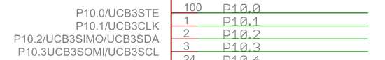
How do I use the CS function on P10.0 ?
Thank you.
