This thread has been locked.

If you have a related question, please click the "Ask a related question" button in the top right corner. The newly created question will be automatically linked to this question.

MSP430G2433: Data written to the microcontroller flash is lost

Part Number: MSP430G2433
Other Parts Discussed in Thread: MSP430G2553

Hi,

we use MSP430G2433 in our Zebra product [MC18 cradle]. we write and read certain memory area in the segment B [2nd segment]. we have a customer who complains that whatever is being written to this area is not being read back, when we read it back, it gives incorrect values.

Need help in resolving this issue on priority as customer operations is impacted due to this issue.

Also, few queries related to the same.

We would like to know details on the below-


  1. Read/Write Endurance cycles
  2. ECC level
  3. MLC or SLC
  4. NOR or NAND flash
  5. Is Flash wear leveling present?
  6. Any Flash controller available?

Thanks,
Vikram

  • Hi Vikram

    Here is some comments from my side

    1. The Read/Write Endurance cycles is 10^4 or 10^5. You can find it at the datasheet chapter 5.35 www.ti.com/.../msp430g2433.pdf
    2&3 I have not find any parameters about that.
    4.NOR flash
    5. Yes.
    6. If your application is at risk of pushing the limits of flash endurance, consider writing a flash
    wear leveling algorithm or switching to one of TI's FRAM-based MSP430 microcontrollers. More information about FRAM www.ti.com/.../slat151.pdf

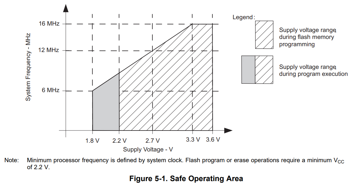
    What's more, could you help me to check if your using condition is under our recommended condition in the datasheet 5.3 that is mainly about power supply and operation frequency. www.ti.com/.../msp430g2433.pdf

    Best regards
    Gary
  • Hi Gary,

    Thanks for the response.

    #2 - ECC - Is there any Error code correction applied on the flash that is part of the micro controller?
    #3 - MLC or SLC - Is the flash that is part of the microcontroller Multi Level Cell or a Single Level Cell or a P-SLC [Pseudo -Single Level Cell]?

    Is there any register or any method to identify if the flash endurance has crossed? what kind of details can we get from the microcontroller?

    As mentioned in my query,
    we use MSP430G2433 in our Zebra product [MC18 cradle]. we have a customer who complains that any write to a particular memory address of INFO segment B was corrupted, any attempts to write to this address was returned success but when read back or debugged it always showed 0x04. I changed the pre-programmed address to the next address cell ( incremented address) which worked and the issue goes away, but it is still unclear why one memory cell of the INFO segment was corrupted ??

    Let me know what details would be needed to for further root causing the issue?

    Need help in resolving this issue on priority as customer operations is impacted due to this issue.
  • Hi Vikram

    I don't find any information about #2&#3.
    I think we don't have any register to identify the endurance. More detail you can refer to www.ti.com/.../slaa334b.pdf
    Have you try information C or D?
    For the flash memory debug information you can refer to this document www.ti.com/.../slaa729a.pdf
    Could you make sure your power supply is stable and above 3.3V? What's MCLK frequency do you use?

    Best regards
    Gary
  • Hi Gary,

    The power supply is stable, MCLK freq is 8MHZ.

    when we write into the INFO segment, how to confirm that write was successful? Any register that could be monitored?

    Also,

    when we write programatically to the flash into a particular address, there are no errors but when this address is read back, it gives a different value, when same address is written via JTAG through CCS the value gets written into the address.  our programatic API works fine and is working in hundreds of devices, we have seen this issue in few devices now.

    let me know what can cause the programatic write fail while it works via JTAG.

    Best Regards,

    Vikram

  • Hi Vikram

    The flash memory is partitioned into main and information memory sections. There is no difference in the operation of the main and information memory sections. Code or data can be located in either section. The differences between the two sections are the segment size and the physical addresses. So there is no registers for the monitored.

    I have try the flash write into the  information  memory C and D with the SBW on MSP430G2553 launchpad and there is no errors here.

    Here is my test code

    /* --COPYRIGHT--,BSD_EX
     * Copyright (c) 2012, Texas Instruments Incorporated
     * All rights reserved.
     *
     * Redistribution and use in source and binary forms, with or without
     * modification, are permitted provided that the following conditions
     * are met:
     *
     * *  Redistributions of source code must retain the above copyright
     *    notice, this list of conditions and the following disclaimer.
     *
     * *  Redistributions in binary form must reproduce the above copyright
     *    notice, this list of conditions and the following disclaimer in the
     *    documentation and/or other materials provided with the distribution.
     *
     * *  Neither the name of Texas Instruments Incorporated nor the names of
     *    its contributors may be used to endorse or promote products derived
     *    from this software without specific prior written permission.
     *
     * THIS SOFTWARE IS PROVIDED BY THE COPYRIGHT HOLDERS AND CONTRIBUTORS "AS IS"
     * AND ANY EXPRESS OR IMPLIED WARRANTIES, INCLUDING, BUT NOT LIMITED TO,
     * THE IMPLIED WARRANTIES OF MERCHANTABILITY AND FITNESS FOR A PARTICULAR
     * PURPOSE ARE DISCLAIMED. IN NO EVENT SHALL THE COPYRIGHT OWNER OR
     * CONTRIBUTORS BE LIABLE FOR ANY DIRECT, INDIRECT, INCIDENTAL, SPECIAL,
     * EXEMPLARY, OR CONSEQUENTIAL DAMAGES (INCLUDING, BUT NOT LIMITED TO,
     * PROCUREMENT OF SUBSTITUTE GOODS OR SERVICES; LOSS OF USE, DATA, OR PROFITS;
     * OR BUSINESS INTERRUPTION) HOWEVER CAUSED AND ON ANY THEORY OF LIABILITY,
     * WHETHER IN CONTRACT, STRICT LIABILITY, OR TORT (INCLUDING NEGLIGENCE OR
     * OTHERWISE) ARISING IN ANY WAY OUT OF THE USE OF THIS SOFTWARE,
     * EVEN IF ADVISED OF THE POSSIBILITY OF SUCH DAMAGE.
     *
     *******************************************************************************
     * 
     *                       MSP430 CODE EXAMPLE DISCLAIMER
     *
     * MSP430 code examples are self-contained low-level programs that typically
     * demonstrate a single peripheral function or device feature in a highly
     * concise manner. For this the code may rely on the device's power-on default
     * register values and settings such as the clock configuration and care must
     * be taken when combining code from several examples to avoid potential side
     * effects. Also see www.ti.com/grace for a GUI- and www.ti.com/msp430ware
     * for an API functional library-approach to peripheral configuration.
     *
     * --/COPYRIGHT--*/
    //******************************************************************************
    //  MSP430G2xx3 Demo - Flash In-System Programming, Copy SegC to SegD
    //
    //  Description: This program first erases flash seg C, then it increments all
    //  values in seg C, then it erases seg D, then copies seg C to seg D.
    //  Assumed MCLK 771kHz - 1428kHz.
    //  //* Set Breakpoint on NOP in the Mainloop to avoid Stressing Flash *//
    //
    //               MSP430G2xx3
    //            -----------------
    //        /|\|              XIN|-
    //         | |                 |
    //         --|RST          XOUT|-
    //           |                 |
    //
    //  D. Dang
    //  Texas Instruments Inc.
    //  December 2010
    //   Built with CCS Version 4.2.0 and IAR Embedded Workbench Version: 5.10
    //******************************************************************************
    
    #include <msp430.h>
    
    char  value;                                // 8-bit value to write to segment A
    
    // Function prototypes
    void write_SegC (char value);
    void copy_C2D (void);
    char arry[70];
    int main(void)
    {
      WDTCTL = WDTPW + WDTHOLD;                 // Stop watchdog timer
    /*  if (CALBC1_1MHZ==0xFF)					// If calibration constant erased
      {											
        while(1);                               // do not load, trap CPU!!	
      }
      DCOCTL = 0;                               // Select lowest DCOx and MODx settings
      BCSCTL1 = CALBC1_1MHZ;                    // Set DCO to 1MHz
      DCOCTL = CALDCO_1MHZ;*/
      FCTL2 = FWKEY + FSSEL0 + FN1;             // MCLK/3 for Flash Timing Generator
      value = 2;                                // initialize value
    
      while(1)                                  // Repeat forever
      {
        write_SegC(value++);                    // Write segment C, increment value
        copy_C2D();                             // Copy segment C to D
        __no_operation();                       // SET BREAKPOINT HERE
      }
    }
    
    void write_SegC (char value)
    {
      char *Flash_ptr;                          // Flash pointer
      unsigned int i;
    
      Flash_ptr = (char *) 0x1040;              // Initialize Flash pointer
      FCTL1 = FWKEY + ERASE;                    // Set Erase bit
      FCTL3 = FWKEY;                            // Clear Lock bit
      *Flash_ptr = 0;                           // Dummy write to erase Flash segment
    
      FCTL1 = FWKEY + WRT;                      // Set WRT bit for write operation
     // value=1;
      for (i=0; i<64; i++)
      {
        *Flash_ptr++ = value;                   // Write value to flash
      }
    
      FCTL1 = FWKEY;                            // Clear WRT bit
      FCTL3 = FWKEY + LOCK;                     // Set LOCK bit
    }
    
    void copy_C2D (void)
    {
      char *Flash_ptrC;                         // Segment C pointer
      char *Flash_ptrD;                         // Segment D pointer
      unsigned int i;
    
      Flash_ptrC = (char *) 0x1040;             // Initialize Flash segment C pointer
      Flash_ptrD = (char *) 0x1000;             // Initialize Flash segment D pointer
      FCTL1 = FWKEY + ERASE;                    // Set Erase bit
      FCTL3 = FWKEY;                            // Clear Lock bit
      *Flash_ptrD = 0;                          // Dummy write to erase Flash segment D
      FCTL1 = FWKEY + WRT;                      // Set WRT bit for write operation
    
      for (i=0; i<64; i++)
      {
        *Flash_ptrD++ = *Flash_ptrC++;          // copy value segment C to segment D
        arry[i]= *Flash_ptrC++;
      }
    
      FCTL1 = FWKEY;                            // Clear WRT bit
      FCTL3 = FWKEY + LOCK;                     // Set LOCK bit
    }
    

  • Hi Gary,

    In general the code is working fine and is being used by many customers, however we have 2 major customers reporting this issue and we are able to see the issue on those units. 

    1. How do we confirm if a flash write is success? as  I see in your sample code as well, the values are written to the memory mapped variables and there is no way to check if the actual write was success or fail?

    2. What scenarios could cause the write via the MSP-FET430UIF pass while the programmatic write [similar to your sample code] fail?

    3. Can we do MARGINAL READ test on MSP430G2433? Is this supported on this microcontroller? Can you share the sample code if its supported?

    4. How do I add my colleagues to this post?

    5. How to engage with TI support to get this investigated so that it can be root caused? 

    Thanks,
    Vikram

  • Hi Vikram
    1. What I do to verify the data are two method (1) use a array to read back from the flash memory (2) write the block D with block C data, if write to the block C data is wrong the data is wrong too in block D.
    2. For the scenarios that can cause the flash memory data corruption you can refer to this document www.ti.com/.../slaa729a.pdf
    3. I don't think MSP430G2433 support this, because I found nothing related to MARGINAL READ in the its datasheet. But I think that is not hard to do it in the code. You just need define a buffer array that located at RAM. You can write the data into the array first and write the data from the array to the flash. Then read back from the flash and compared with the array. If it is same that is OK, if it is not write the flash again.
    4. Your colleagues can response to this post directly
    5. I will keep to follow this issue

    Best regards
    Gary
  • Hi Gary,

    Can you provide details and insight into why would the write via the MSP-FET430UIF pass while the programmatic write [similar to your sample code] fail?

    what is the difference between programatic write vs the write that happens via MSP-FET430UIF [we put a breakpoint and modified the value in
    the memory browser in CCS and then we could see that it was written into the problematic address]

    We see that, we can edit memory location directly from the memory browser in the CCS, and have it reflected correctly when we read from the data back.
    It is actually when we write something, it is not written to the corrupted(assumed) memory locations.

    We did a bit of exercise to understand the pattern of the failures,
    Erase once and Read continuously - Not all bytes are 0xFF, but read seems to be consistent.
    Write, Read back and compare the values.
    Have Delay between writes of each byte in writing the complete segment.

    In all the cases we see, reading the values is consistent, it fails to erase and write programatically.

    Thanks,
    Vikram
  • Vikram,
    Can you share the firmware code that writes to FLASH?

    Can you try a memory write test on suspect unit(s)? See below.
    Since it is INFO memory, I'm assuming your working units are doing the WRITE correctly. i.e. unlocking the segment first.
    Can the issue be 100% reproduced on the suspect unit(s)?

    ============================================================================
    void write_SegA (char value)
    {
    int *Flash_ptr; // Flash pointer
    unsigned char i;

    Flash_ptr = (int *) 0x1080; // Initialize Flash pointer
    FCTL1 = FWKEY + ERASE; // Set Erase bit
    FCTL3 = FWKEY; // Clear Lock bit
    *Flash_ptr = 0; // Dummy write to erase Flash segment

    FCTL1 = FWKEY + WRT; // Set WRT bit for write operation

    for (i=0; i<128; i++)
    {
    *Flash_ptr++ = value; // Write value to flash
    }

    FCTL1 = FWKEY; // Clear WRT bit
    FCTL3 = FWKEY + LOCK; // Set LOCK bit
    }

    Be carefull when using SegmentA since the calibration constants were stored there! Have a look at the post e2e.ti.com/.../24510.aspx ; I've posted an example there which can be used for accessing all INFO memory segments. Because you use a variable as argument the function will access (erase) the memory segment in which this variable is stored.
  • Hi,

    Code is exactly same as Gary shared earlier in this forum. Please share your mail id, if you need to see complete code.

    void flash_write_byte(const memaddr8_t mem_addr_index, volatile unsigned char *inBuffer)
    {
    writeAddr = 0xAAAA; //Hardcoded zone address for the particular byte
    _disable_interrupts();
    //Backup the entire segment of 64 bytes in temp buffer in RAM

    //Modify temp buffer with the input bytes coming from inBuffer

    flash_erase_open(); // FCTL3 = FWKEY;FCTL1 = FWKEY + ERASE;
    *writeAddr = 0;
    flash_erase_close(); //FCTL3 = FWKEY + LOCK;

    // 2 clock cycles stabilization time
    _no_operation();_no_operation();

    flash_write_open(); // FCTL3 = FWKEY;FCTL1 = FWKEY + WRT;

    //copy modified temp buffer to flash addr 'writeAddr' in loop
    for (i=0; i<64; i++)
    {
    *writeAddr++ = value; // Write value to flash
    }

    flash_write_close(); // FCTL1 = FWKEY;FCTL3 = FWKEY + LOCK;

    _enable_interrupts();
    }

    Data written to *writeAddr programitically, does not persist in flash, however if we change the value from memory browser of CCS, value is persisted, and same value is read back consistantly.

    Issue is 100% reproducible in infected units, but the same code is working in majority of other devices correctly.

    If we shift the address of bytes written, then we don't see the problem anymore, In the sense problem appears to be for specific bytes in memory.

    Thanks,

    Rajat

  • Hi,


    Code is exactly same as Gary shared earlier in this forum. Please share your mail id, if you need to see complete code.


    void flash_write_byte(const memaddr8_t mem_addr_index, volatile unsigned char *inBuffer)

    {

                   writeAddr = 0xAAAA; //Hardcoded zone address for the particular byte  

                   _disable_interrupts();    

                    //Backup the entire segment of 64 bytes in temp buffer in RAM


                    //Modify temp buffer with the input bytes coming from inBuffer


                    flash_erase_open(); // FCTL3 = FWKEY;FCTL1 = FWKEY + ERASE;

                    *writeAddr = 0;                

                    flash_erase_close(); //FCTL3 = FWKEY + LOCK;


                    // 2 clock cycles stabilization time

                   _no_operation();_no_operation();


                   flash_write_open(); // FCTL3 = FWKEY;FCTL1 = FWKEY + WRT;


                   //copy modified temp buffer to flash addr 'writeAddr' in loop

                   for (i=0; i<64; i++)

                   {

                                  *writeAddr++ = value; // Write value to flash

                   }


                   flash_write_close(); // FCTL1 = FWKEY;FCTL3 = FWKEY + LOCK; 


                   _enable_interrupts();

    }


    Data written to *writeAddr programitically, does not persist in flash, however if we change the value from memory browser of CCS, value is persisted, and same value is read back consistantly.


    Issue is 100% reproducible in infected units, but the same code is working in majority of other devices correctly.


    If we shift the address of bytes written, then we don't see the problem anymore, In the sense problem appears to be for specific bytes in memory.

  • Hi Vikram

    What do you mean by "Issue is 100% reproducible in infected units"?

    What's the percentage of the infected units?

    Dose the certain memory area in the segment B is the same address? 

    What's the versions of the infected units?

    Best regards

    Gary

  • Vikram Murthy said:

    We would like to know details on the below-


    1. Read/Write Endurance cycles
    2. ECC level
    3. MLC or SLC
    4. NOR or NAND flash
    5. Is Flash wear leveling present?
    6. Any Flash controller available?

    Sigh..

    It is obvious that the TI part has defective ECC and wear leveling system for the flash storage.

    This is not a surprise since there is no dedicated hardware for these features

    Any wear leveling and error correction must be provided by customer code.

    Good luck

  • Hi Gary,

    we have few customer units where issue is always reproducible, it means that the 2 bytes that we use in INFO segment B is having write issues, write to these 2 bytes fails when we try to write programmatically and this is impacting customer use case. interestingly if we write to those 2 bytes using the MSP debugger via CCS [we modified those 2 addresses in the memory browser] it gets written successfully, but again after this if we try to write to those addresses again via programatically it fails again.

    we have 2 units with us received from customer and we can see this issue, customer has more units that exhibit this issue.

    can you tell us why programatic write failed while it worked via the MSP debugger, what is the difference between these 2 methods? let us know if there is any register to be checked to determine the write failures.  the other bytes in the segment is fine.

    Thanks,

    Vikram

  • Hi Vikram

    I will report this issue to our tools team and response to you if any update here.

    Best regards

    Gary

  • Hi Gary,

    Also, Is there any recommended time delay between successive read/writes issued to the micro-controller? 

    Thanks,

    Rajat

  • Hi Rajat

    I have not try the delay, because there is no problem from my side.

    Could you help me to sand some bad devices to me? I have sent you my email address before. You can connect me by the email.

    Best regards

    Gary

  • Thanks Gary.

    We will update you about the failed cradles, as they are in customer possession. We also wanted to know if it is safe if we use Segment D, as a mitigation to the problem? I mean if in any way, stressing segment C, would hamper segment D as well? I can see Segment D is untouched programitically,  but segment C is used for a while now and we see wrong data read from Segment C only.

    Thanks,

    Rajat

  • Also, we see that JTAG read/writes are more stable then done programitically? Can we know what could be the difference, is this a timing related thing?

    Thanks,

    Rajat

  • Hi Rajat

    What's power voltage do you use? You just say it is stable but not mention what's the voltage value. What I want to do is to confirm your operation is in safe area

  • Hi Gary,

    Please find the input voltage range.

    Channel : INCH_11
    ADC10AE0 |= BIT3 + BIT0;
    ADC10CTL1 = SHS_0 + ADC10SSEL_0 + ADC10DIV_2 + CONSEQ_2 + channel;
    ADC10CTL0 = SREF_1 + ADC10SHT_3 + REF2_5V + REFON +ADC10ON;

    #define MCU_VOLTS_MIN_ADC_VALUE 637
    #define MCU_VOLTS_MAX_ADC_VALUE 715

    Write operates between MCU_VOLTS_MIN_ADC_VALUE  and MCU_VOLTS_MAX_ADC_VALUE  only. So if there is a voltage variation, it is detected as an error, which is not in our case.

    Thanks,

    Rajat

  • Hi Rajat

    What I want to check is the voltage of the VCC not the input of the ADC. What I show you the picture is the relation between MCLK frequency and VCC voltage.

    Best regards

    Gary

  • Hi Rajat

    Any update about that? 

    Best reagards

    Gary

**Attention** This is a public forum