Hello All,
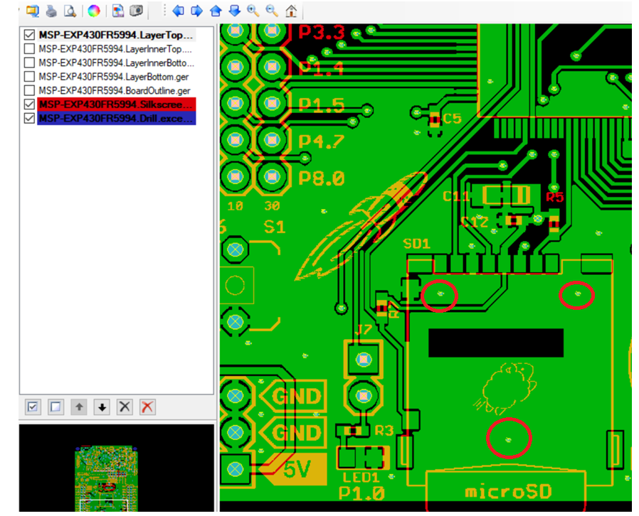
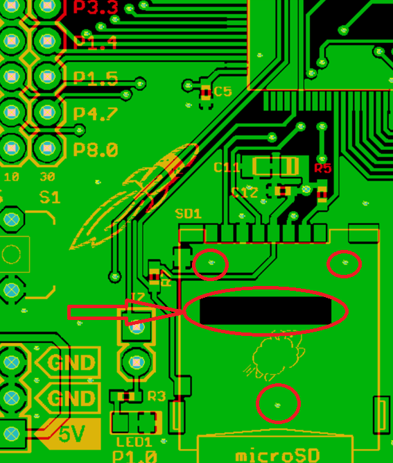
The Gerber Layout appear inconsistent with the schematic representation wrt to the Micro SDCard.
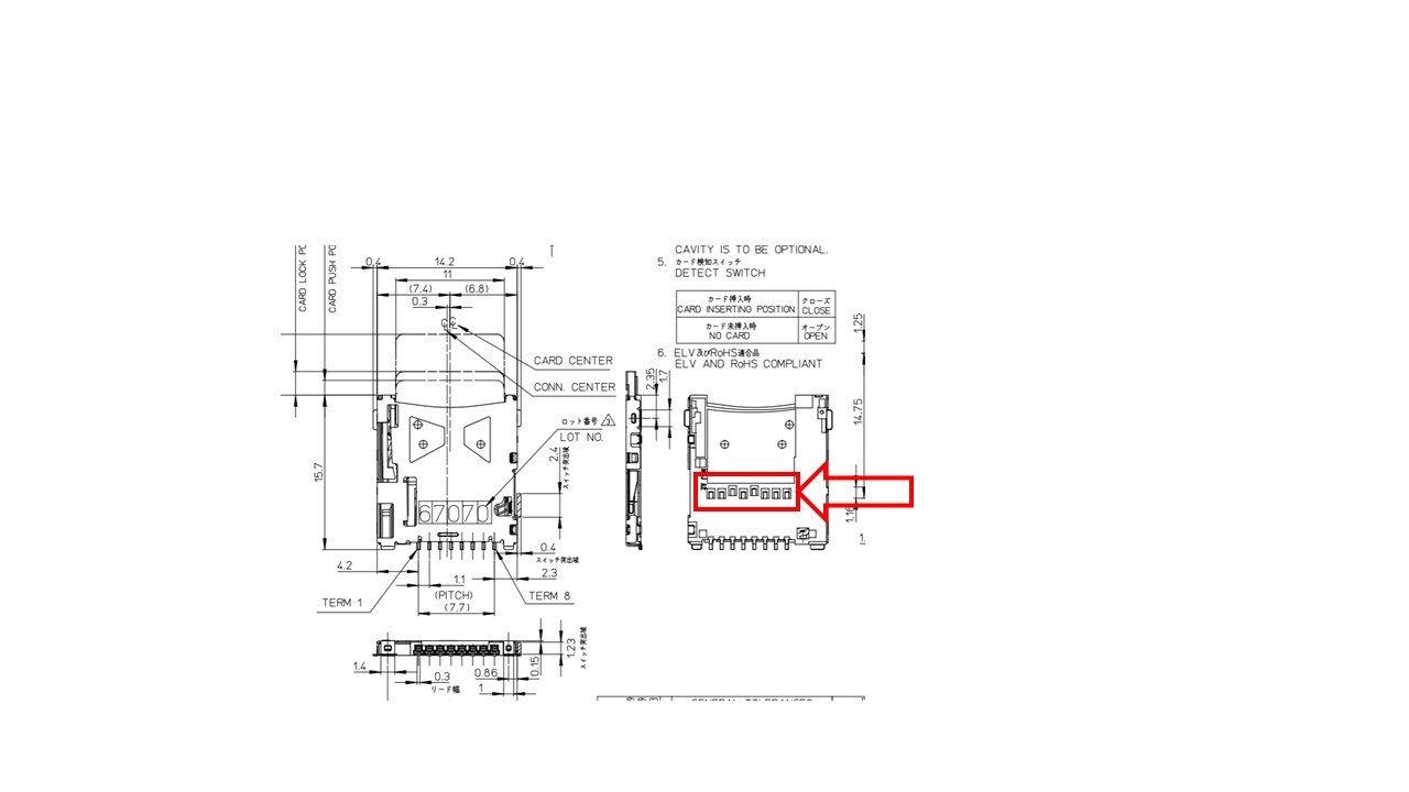
- The pdf schematic (2nd image below) shows that the P2.7_SD_Detect signal is attached to a "pin B" of the device. The layout gerbers show P7.2_SD_Detect connected to pin 4. The datasheet for the SDCard (Molex) does not provide a circuit diagram for the 10 pin part so I do not know what functions pin A and pin B provide. Can anyone help here and explain this apparent inconsistency.
- Pin A is grounded on the schematic. The Gerber files show a grounded landing pad next to the R7 resistor which connects to the SD socket. Is that pin A?
- From the Gerbers, it appears that the case is not grounded.
- And can anyone tell me why is there an opening in the Top Metal (green) under the SDCard socket?
thank you for any help
jjim


