This thread has been locked.

If you have a related question, please click the "Ask a related question" button in the top right corner. The newly created question will be automatically linked to this question.

MSP430FR2355: How to trigger ADC12 sampling sequence from TB1.1

Part Number: MSP430FR2355


Hi

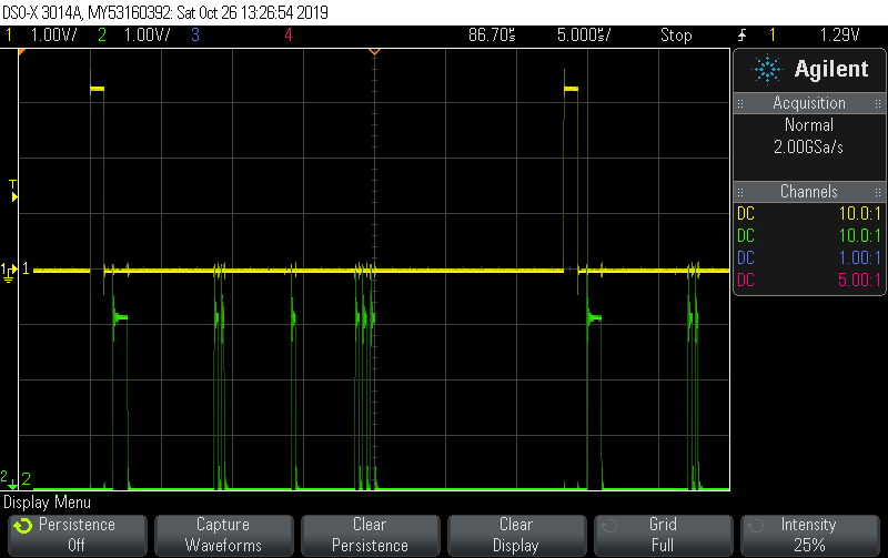
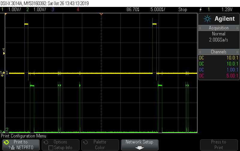
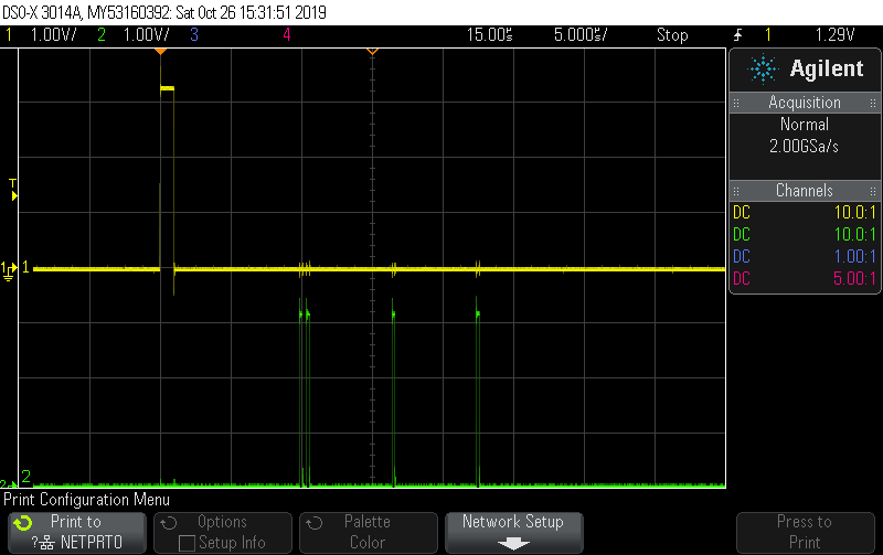
I am trying to figure out how to use timer1 (TB1.1) to trigger sample and convert of 3 sequential analog channels (A0-A3).

As indicated in table 6-22 of the data sheet, Selecting ADCSHSx=0x2 should trigger the sampling sequence.

However, when looking at SLAU445i section 21.2.7.2 figure 21-13 (sequence of channels, 12bit), there is no TB1.1 signal in the flow diagram to trigger the sequence rather you should flip some SW bits in order to start a new sequence. (according to chart you need a rising edge on ADCENC to start a new sequence !!!)

1) is there a detailed explanation on how TB1.1 triggers a sequence.

2) Is there a SW code example that shows how to trig a new sequence from TB1.1 without the need for flipping a SW bits inside an interrupt routine?

Best regards

Ofer Zilberberg

  • 1) The key word in Fig 21-13 is "Trigger". That's SHS (TB1.1 in your case).

    2) No. There's no way to use CONSEQ=1 with SHS > 0 without toggling ENC on every burst. If you don't need bursting behavior (the signals are uncorrelated, so they don't need to be sampled quasi-simultaneously) you can use CONSEQ=3 with MSC=0 and multiply your timer frequency by 4. As a practical matter, you need intra-burst spacing anyway to give you time to pick up the samples from MEM0.

  • Dear Bruce

    thank you for your replay.

    I am still puzzeled regarding the exact way TB1.1 is used for triggering.

    1) in your answer to #1 - how does TB1.1 involved in "triggering", Looking in Figures  21-10 to 21-17 on SLAU445i, does not revile how TB1.1 is involved in triggering. Can you elaborite on it?

    2) As for you answer to #2 - Do you mean that TB1.1 have any influance on the triggering when using CONSEQ=3 with MSC=0? does it trigger each individual conversion?
        Again, it is not clear to me how TB1.1 is involved. Can you try to explain, since i cant find any explanation on the WEB?

    Regards

    Ofer Zilberberg

  • 1) TB1.1 provides a waveform (OUTMOD) where the rising edge of the signal is the Trigger -- it serves as SHI in UG Fig. 21-6. (With SHP=0, the ADC uses the falling edge of the TB1.1=SHI waveform to stop the sample/hold phase, rather than counting by SHT on its own, Ref Fig 21-5.)

    OUTMOD=7 or =3 is usually a good choice. (I prefer =7 since triggering at the beginning of the timer cycle helps me keep my head straight.)

    2) Yes, with MSC=0 each Trigger does one conversion -- thus the need to increase your timer frequency so you get all the samples within the intended cycle time. But CONSEQ=3 gets you out of the ENC-toggling business. 

    And, as I mentioned, you need to look ahead to understand how you're going to fetch each sample from MEM0 before the next one arrives. (Only one MEM register, no DMA.) MSC=0 can help with that as well.

  • Hi Bruce

    Thank you very much for your help, it is starting to work except i dont get ~200Ksps from the ADC. instead i have ~30 uS between sequential conversions.

    I am using 24Mhz Sclk and initiate TB1 for:

    TB1CCR0 = 3600-1; // CCR0 will contain the PWM Period , defining the max counting value for the TB.

    TB1CCTL1 = CLLD1 | OUTMOD_7; // TBxCLn loads when TBxR counts to 0 (up or continuous mode). TBxCLn loads when TBxR counts to TBxCL0 or to 0 (up/down mode).
    // , CCR1 set/reset (CCR0=set CCR1=reset)
    TB1CCR1 = 24; // CCR1 ADC start convert and PWM duty cycle
    TB1CCTL2 = CLLD1 | OUTMOD_7; // CCR2 reset/set (CCR2=reset CCR0=set)
    TB1CCR2 = 700; // CCR2 PWM duty cycle
    TB1CTL = TBSSEL__SMCLK | MC__UP | TBCLR | TBIE; // SMCLK, up mode, clear TBR, add | TBIE to Enable timer interrupt. note the upper bits are zero to indicate "no group" and 16 bit operation.

    note: TB1.1 Interupt is used only for DAC output update and is not part of ADC operation.

    for the ADC init: (Exuse me for the large amount of comment - i am a beginner).

    ADCCTL0 = 0; // Disable ADC conversion to enable registers change.
    ADCCTL0 |= ADCSHT_0 | ADCMSC | ADCON; // ADC sample-and-hold time=1 x 4x ADCclk, ADC multiple sample-and-conversion enabled,ADC turn ON
    ADCCTL1 = ADCSHS_2 | ADCSHP | ADCDIV_5 | ADCCONSEQ_1 ;//  Trig on TB1.1 ,use non invert of TB1.1 in order to sample , FOR MCLK=24Mhz use ADCDIV_5 (ADCclk = SMclk/6); to enable ADCclk <=4.4Mhz for 12 bit (6Mhz for 10bit), repeat single sequence of channels.
    ADCCTL2 = ADCRES_2; // 12-bit conversion results
    ADCMCTL0 = ADCINCH_2 | ADCSREF_1; // internal Vref 2.5v, start sequence at A2 (down to A0)

    ADCIE |=ADCIE0; // Enable the Interrupt request for "end of conversion"

    // Configure reference
    PMMCTL0_H = PMMPW_H; // Unlock the PMM registers
    PMMCTL2 |= INTREFEN | REFVSEL_2; // Enable internal 2.5V reference
    __delay_cycles(400); // Delay for reference settling
    ADCbuffull = 0; // initiate "ADC buffer full" flag to empty (used for temporary ADC buffer)
    ADCCTL0 |= ADCENC; // Enable ADC conversion

    In order to get the ADC results i am using a temporary 3 words array (ADC_result)  and therefore inside the ADCIFG (ADC interupt) i have the code:

    case ADCIV_ADCIFG:
    ADC_Result[(ADCMCTL0 & 0xF)] = ADCMEM0; //A0 reading into ADC_Reseul[0],A1 reading into ADC_Reseul[1],A2 reading into ADC_Reseul[2]
    // note the usage of the actual "channel select bits" of the ADC as an index for temporary buffer storage.
    // ADC_Result[(ADCMCTL0 & 0xF)] |= ((ADCMCTL0 & 0xF)<<12); // option to Add channel No. at MSB.

    if((ADCMCTL0 & 0xF) == 0) // When last ADC channel in the sequence was sampled
    {
    ADCbuffull = 1; // change indication of "ADC buffer full" flag to full.
    ADCCTL0 &= ~ADCENC; // Disable ADC conversion
    ADCCTL0 |= ADCENC;    // Enable ADC conversion.
    }
    P6OUT ^= BIT6; // Toggle P6.6 using exclusive-OR

    ADCIFG = 0; // Clear interrupt flag
    break;

    This work well except for 2 problems:

    1) Since i am toggeling a bit in each ADC interrupt, i have mesured the sequencial convertion time to be ~30uS which is 33K samples per seconds - very low.
    What can i do, why it is hapening.

    2) My ADC_result[2] =0 always. indicating somthing wrong with A2 conversion. Please note i can see 3 toggeling of P6.6 folowing every pulse of TB1, which indicate the ADC do convert A2,A1,A0.

    Can you think on an answer to my 2 questions.

    Thanks in advance.

    Ofer Zilberberg

  • 2) For CONSEQ=1, INCH is updated right after the conversion is done, so it reflects the Next channel to be converted. Corollary: When the sequence completes, INCH stays at 0, so reading INCH==0 is ambiguous. For CONSEQ=1, it's probably better to use a global counter variable.

    1) With SMCLK=24MHz and CCR0=3600, you're requesting 24000000/3600=6666 triggers/sec. Each trigger gives 3 samples, so that's 20ksps.

    With ADCSSEL=0 and ADCDIV=5, your ADC clock is 3800000/6=633333Hz. [MODOSC assumed 3.8MHz per datasheet (SLASEC4B) Table 5-9]

    With SHT=0, each conversion takes 4+14+1=19 ADC clocks [Ref UG (SLAU445I) Fig 21-13]. So your burst sampling rate is 633333/19=33333 sps, Which is about what you're measuring.

    You can reduce your per-conversion time by decreasing ADCDIV. Your throughput is currently limited by your trigger period (CCR0).

    [Edit: Fixed typo.]

  • Hi Bruce

    Thanks again for the prompt replay.

    As for question 1  - i have discovered i forgot to add ADCSSEL_2 setting in the ADCCTL1 register.

    Now i get ~5uS between samples and this is OK.

    As for question 2 - you are correct, by the time the SW deal with the ADC interrupt, the channel counter was updated and will point to the next channel, so i assumed that instead of reading A2,A1,A0 - i will have all with one shift.

    So in each sequence i will have 3 readings of A1,A0,A2 (all the 3 channels only shifted by sequence).

    In order to understand what is happening i have added different to gelling on P6.6 (3 short pulses to indicate A2, 2 short pulses to indicate A1 and 1 short pulse to indicate A0).

    Attached find file ADCIFG.c with the code for your convenience.

    // ADC interrupt service routine
    #if defined(__TI_COMPILER_VERSION__) || defined(__IAR_SYSTEMS_ICC__)
    #pragma vector=ADC_VECTOR
    __interrupt void ADC_ISR(void)
    #elif defined(__GNUC__)
    void __attribute__ ((interrupt(ADC_VECTOR))) ADC_ISR (void)
    #else
    #error Compiler not supported!
    #endif
    {
        switch(__even_in_range(ADCIV,ADCIV_ADCIFG))
        {
            case ADCIV_NONE:
                break;
            case ADCIV_ADCOVIFG:
                break;
            case ADCIV_ADCTOVIFG:
                break;
            case ADCIV_ADCHIIFG:
                ADCIFG &= ~ADCHIIFG;            // Clear interrupt flag
                break;
            case ADCIV_ADCLOIFG:
                ADCIFG &= ~ADCLOIFG;            // Clear interrupt flag
                break;
            case ADCIV_ADCINIFG:
                break;
            case ADCIV_ADCIFG:
                ADC_Result[(ADCMCTL0 & 0xF)] = ADCMEM0; //A0 read into ADC_Reseul[0],A1 reading into ADC_Reseul[1],A2 reading into ADC_Reseul[2]
                                // note the usage of the actual "channel select bits" of the ADC as an index for temporary buffer storage.
                if((ADCMCTL0 & 0xF) == 2)   // When last ADC channel #2 in the sequence was sampled
                {
                  P6OUT ^= BIT6;
                  P6OUT ^= BIT6;
                  P6OUT ^= BIT6;
                  P6OUT ^= BIT6;
                  P6OUT ^= BIT6;
                  P6OUT ^= BIT6;   // Toggle P6.6 x 6 times to to create 3 short pulses for distinguish on SCOPE.
                }
                if((ADCMCTL0 & 0xF) == 1)   // When last ADC channel #1 in the sequence was sampled
                {
                  P6OUT ^= BIT6;
                  P6OUT ^= BIT6;
                  P6OUT ^= BIT6;
                  P6OUT ^= BIT6;   // Toggle P6.6 x 4 times to to create 2 short pulses for distinguish on SCOPE.
                }
                if((ADCMCTL0 & 0xF) == 0)   // When last ADC channel #0 in the sequence was sampled
                {
                  P6OUT ^= BIT6;
                  P6OUT ^= BIT6;   // Toggle P6.6 x 2 times to to create 1 short pulse for distinguish on SCOPE.
                  ADCbuffull = 1;         // change indication of "ADC buffer full" flag to full.
    
                  ADCCTL0 &= ~ADCENC;     // Disable ADC conversion
                  ADCCTL0 |= ADCENC;      // Enable ADC conversion.
    
                  ADCIFG = 0;            // Clear interrupt flag
                }
                break;
            default:
                break;
        }
    }
    

    I have added additional toggling for long pulse on TB1 interrupt routine (file TB1IFG.c):

    // Timer1_B3 Interrupt Vector (TBIV) handler
    // init during ADC_TB1_init.c
    // used for writing DAC values.
    #if defined(__TI_COMPILER_VERSION__) || defined(__IAR_SYSTEMS_ICC__)
    #pragma vector=TIMER1_B1_VECTOR
    __interrupt void TIMER1_B1_ISR(void)
    #elif defined(__GNUC__)
    void __attribute__ ((interrupt(TIMER1_B1_VECTOR))) TIMER1_B1_ISR (void)
    #else
    #error Compiler not supported!
    #endif
    {
        switch(__even_in_range(TB1IV,TB1IV_TBIFG))
        {
            case TB1IV_NONE:
                break;                               // No interrupt
            case TB1IV_TBCCR1:
                break;                               // CCR1 not used
            case TB1IV_TBCCR2:
                break;                               // CCR2 not used
            case TB1IV_TBIFG:
                P6OUT ^= BIT6;          // Toggle P6.6 using exclusive-OR
                DAC_data++;
                DAC_data &= 0xFFF;
                SAC3DAT = DAC_data;     // DAC12 output positive ramp
                P6OUT ^= BIT6;          // Toggle P6.6 using exclusive-OR to indicate "end of TB1IFG".
                break;
            default:
                break;
        }
    }
    

    In addition i have changed the CC0 timer to 800 since i solved the #1 question :) .

    I assumed to get on the scope a picture of: (where upper yellow trace is P2.0 (TB1.1) output, and lower green trace is P6.6):

    But i was surprised to find out that only rarely i get this picture (taking multiple snapshots with the scope), in most of time i get this:

    Indicating missing sample of channel A2.

    I have no clue of what is happening - can you help?

    Best regards

    Ofer Zilberberg

  • Sorry, yes you're right about INCH being re-set at the end. I must have been thinking about some other chip.

    The things I'm looking at:

    1) If a conversion takes 5usec, that's how long you have to pick up MEM0. That's about 5*24=120 CPU clocks. That sounds like a lot, but it goes quickly, and I would say your ISR is a bit on the heavy side.

    This sets up a race. Your ISR can drift forward in time without incident (you can kind of see that in the scope trace) until it overruns something.

    2) You're doing the ENC toggling when INCH==0, which is (nominally) during the conversion of channel 0. Depending on how the race in (1) above is running, this might or might not actually be during the conversion. UG Sec 21.2.7.6 makes this sound benign, but I'm not sure I would want to push it.

    3) Are you using LPM? The wakeup times can make a difference when you're pushing the limits.

    ------

    If I were doing forensics, I'd dig through the assembly code and see what cases could arise. Since you're still in development, I'd say "Fix: Avoid". I.e some subset of:

    A) Measure how long your ADC ISR takes, e.g. by wiggling a GPIO on entry and exit. Since you're using ^= on P6.6 you might be able to get triple-duty out of it.

    B) Lighten up your ADC ISR

    C) Do the ENC toggling when INCH==2

    D) Slow down your ADC conversions just slightly (plus some Engineering margin).

  • Update

    I have figure up that i probably have a problem with the time it takes the ADC interrupt to execute, compared with the time of the ADC conversion sequence.

    I have slow down the conversion sequence time by enlarging the sample time (using ADCCTL0 |= ADCSHT_1 | ADCMSC | ADCON; instead of ADCCTL0 |= ADCSHT_0 | ADCMSC | ADCON;).

    I have also eliminate completely the TB1 interrupt leaving only the ADC interrupt running.

    Now i get stable 3 sequential readings but not in the correct order:

    Apparently, channel A0 is converted 2 times.

    How can it happened without a sync ? (i have tried to enlarge the sampling time with same results).

    Thanks in advance

    Ofer Zilberberg

  • How long does your ADC ISR actually take?

    Are you still toggling ENC when INCH==0?

  • Hi Bruce

    Thank you for the prompt answer - it helps to solve the case.


    1) I have used a global counter for the channel count as you suggested.

    2) Apparently X=inchx does not performed as the flow chart suggested, rather after flipping the EMC bit, therefore I have located another interrupt (Using CCR2) to be placed  after the 3 conversions to take care of the flipping, leaving the ADCISR only with storing the MEM0 data.


    I achieve 5uS between samples (7usec from the TB1.1 to first ADCINT and 5uS after that).


    Thank you for your patience and deep understanding, May the force be with you :)   .


    Best regards

    Ofer Zilberberg

**Attention** This is a public forum