This thread has been locked.

If you have a related question, please click the "Ask a related question" button in the top right corner. The newly created question will be automatically linked to this question.

CCS/MSP430G2553: How the timer initialization done in “DRV8313EVM_RevB”.

Part Number: MSP430G2553
Other Parts Discussed in Thread: DRV8313EVM, DRV8313,

Tool/software: Code Composer Studio

Dear sir

I am currently working on an application to run a simple program on my sensorless BLDC motor using DRV8313EVM module (48V, 35watt). I would like to run the motor in standalone mode with a certain set of algorithms with DRV8313.

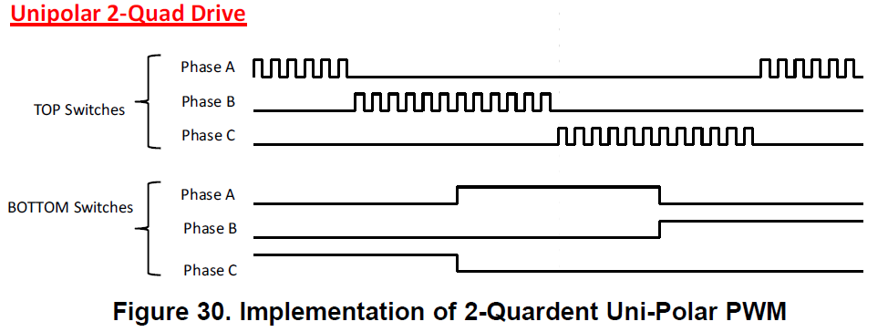
I am not able to understand how the bottom switches pulse generates with which timer? The DRV8313EVM is used. The file attached here is from slvu815a.pdf, “ DRV8313EVM User’s Guide”.

The timer initialization code is given below in “DRV8313EVM_RevB”.

void Init_Timer (void)

{

       TA1CCR0 = 400;             // Load the Reference Count

       TA1CCTL2= OUTMOD_6;

       TA1CCR2= (100-START_UP_DUTY) * 4;

       TA1CTL =TASSEL_2 + MC_3 + TACLR ; //+TAIE;//Up-Down Mode ,SMCLK,Timer Clear

        TACCR0 = 400; // Load the Reference Count

       TACCTL0= CCIE;

       TACCTL2= OUTMOD_6;

       TACCR2 = 398;

       TACTL  = TASSEL_2 + MC_3 + TACLR ;

             //+ TAIE;    //Up-Down Mode , SMCLK , Timer Clear


       WDTCTL = WDT_MDLY_32;

       IE1    |= WDTIE;                         // enable WDT interrupt

       _EINT();                             // Enable interrupts

}


I am quite new to programming with MSP430. Appreciate any advice/help, 

Thanks,

Ajeet

  • Hello,

    I'm not familiar to DRV8313 2-Quardent Uni-Polar drive mode. But according to the timer initialization code, the Timer A0 Compare channel 2 and Timer A1 Compare channel 2 to generate PWM at pin TA0.2 and TA1.2. Please see the MSP430G2x53, MSP430G2x13 Mixed Signal Microcontroller datasheet (Rev. J) and MSP430x2xx Family User's Guide (Rev. J) Timer A module for more information. 

  • Dear Sir,

    Thanks, this is the MSP430G2553 code issue, 

    Using timer TA1.2, 3-PWM signal generated by the ports P2.4, P2.5, P3.3, it's fine and TA0.2 is used for P3.0

    But how P3.1, P3.2 generates the active signals pulse? Not able to understand with the above timer initialization code.

    Regards

    Ajeet

  • Hello,

    I checked the DRV8313 datasheet and the schematic of DRV8313EVM.

    It seems that the DRV8313 doesn't support separated control for high side and low side switch. The states of each leg are high, low and Hi-Z which are controlled by the INx and ENx signal.

    So I think the active signal on bottom side doesn't mean PWM pulse. It means a ON state. The 2-Quardent Uni-Polar drive mode is implemented by the PWM on INx lines and signal on ENx lines. Just like the trapezoidal commutation described in DRV8313 datasheet. 

  • Thanks for detail of DRV8313, 

    But my question is how to generate the signal on ENx lines ? and how the MSP430G2553 Pin 3.0, 3.1, 3.2 generates the signal for ENx lines. Which timer is used

    Regards

    Ajeet

  • Hello,

    To generate high/low signal, you can use the pin as GPIO output function. Take P3.0 as example,

    P3DIR |= BIT0;   // Set as output

    P3OUT |= BIT0; // Output high

    P3OUT &= ~BIT0; // Output low

    To generate PWM signal, the pin need a Timer PWM out function, such as TAx.y. x and y represents x Timer A module and y channel.

           TAxCCR0 = period;             // Set PWM period

           TAxCCTLy = OUTMOD_6; // Set PWM output mode

           TAxCCRy = duty;               // Set PWM dutycycle

           TAxCTL =TASSEL_2 + MC_3 + TACLR ; // Up-Down Mode, SMCLK, Timer Clear

  • Thanks sir

    Also, I am not able to understand, in DRV8313 EVM given program,

    In EVM Back emf sensed but in the code only VDC bus sense, so how the Insta_Spin.h is working without back emf voltage.

    void Init_ADC ()
    {
    ADC10CTL0 |= SREF_1 + ADC10SHT_2 + ADC10ON + ADC10IE + REFON + REF2_5V;
    ADC10CTL1 = INCH_6 + CONSEQ_0 + ADC10SSEL_2 ; // Sequence of channels upto A6
    ADC10AE0 |= 0x40;
    }

    Regards

    Ajeet

  • Hello,

    I checked the schematic. It should sense channels A0-A6 with sequence of channels mode. It seems the given ADC initialization code wants to configure the ADC to sequence of channels upto A6. But actually, it couldn't achieve that with CONSEQ_0 setting. It should be 

    ADC10CTL1 = INCH_6 + CONSEQ_1 + ADC10SSEL_2 ; // Sequence of channels upto A6

     Could you check if the code configures the ADC conversion mode in other place?

  • Great Improvement in BLDC motor running performance with this change (CONSEQ_0 => CONSEQ_1 ), please correct in the main program in DRV8313EVM software.

    Please also clarify, how the sensed 3-phase  back emf linked to the Insta_spin.h file, for implement the instaspin algorithm? while no adc variable defined in main.c code.

    Regards

     Ajeet

  • Thanks for your findings.

    Sorry, the DRV8313EVM software is developed by motor driver product line. From MSP430 side, I only can clarify the application of peripheral modules of MSP430. I'm not familiar to the instaspin algorithm. 

    Could you post remained question about instaspin algorithm in motor driver forum and let them know the bug in code?

**Attention** This is a public forum