In the source code of our products, we have a line that confuses me:
CAPD = CAPD4;
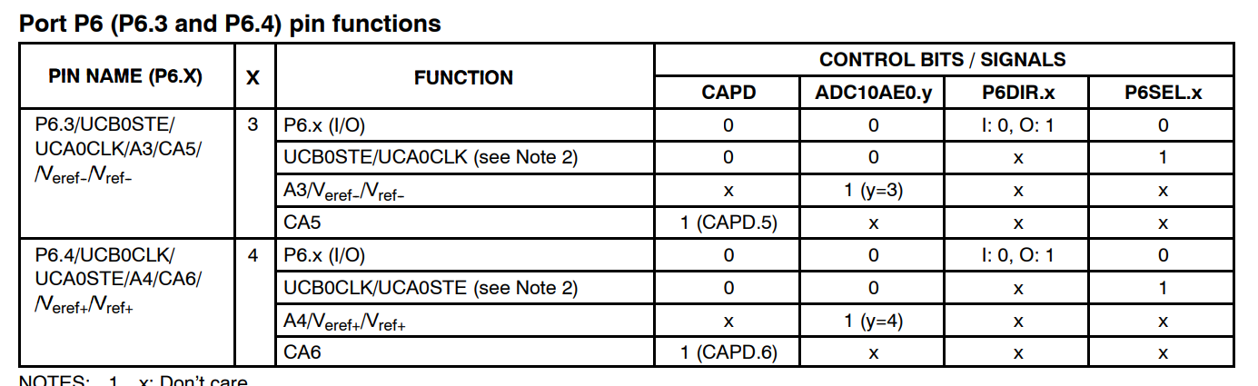
All our products with MSP430F41x2 have had this line of code for many years. The code doesn't seem to match our hardware. Here is an example hardware configuration
// P1.6 - CA0 (not connected)
// P1.7 - CA1 (not connected)
// P7.4 - CA2 (-terminal of Comparator A)
// P7.5 - CA3 (digital output)
// P6.0 - CA4 (ADC input)
// P6.3 - CA5 (not connected)
// P6.4 - CA6 (+terminal of Comparator A, reference output)
// P6.7 - CA7 (ADC input)
If my understanding of the family user guide is correct, then we should disable i/o buffer for CA2 and CA6, so the code should probably look like
CAPD = CAPD2 | CAPD6;
Can someone please clarify how to decide which bit of CAPD should be set?