This thread has been locked.

If you have a related question, please click the "Ask a related question" button in the top right corner. The newly created question will be automatically linked to this question.

MSP430FR5989-EP: Unexpected CPU delay when triggering DMA

Part Number: MSP430FR5989-EP
Other Parts Discussed in Thread: MSP430FR5989, MSP430FR6989

Hi,

I´m having an unexpected behaviour signaled by MCLK, working with a MSP430FR5989EP Rev.E, that I need to better understand before designing any workaround.


Context:

The microcontroller periodically receives an asynchronous SPI communication in 4-pin slave mode that represents a status message from the master.
The SPI reception triggers DMA1 module configured in single mode byte transfer to move each of the N received bytes (status message has a known fixed length N) from UCB0RXBUF to a buffer in RAM (incrementing destination also as byte), to be processed in main routine after the DMAIFG is raised.
The microcontroller's main loop periodically waits in LPM3 mode for a TimerA0.0 interrupt while SPI reception can occur, and many times the TimerA0.0 ISR overlaps with SPI reception without problem.
But there is a specific scenario, that makes DMA module to lately transfer a byte of such status message.

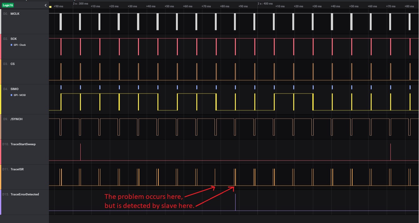
The following picture (PICTURE1) is a capture of the SPI reception (SCK and SOMI signals) attended by DMA module as short MCLK signal bursts (0.625us width) approx. 5us after the 8th risig edge of SCK, that overlaps with execution of the main routine attending Timer A0.0 interrupt and returning to LPM3 (TRACE1 signal).

PICTURE1: https://drive.google.com/file/d/1_sZtCb4t-Eim0TyWaygotPmCtsETUFln/view?usp=sharing

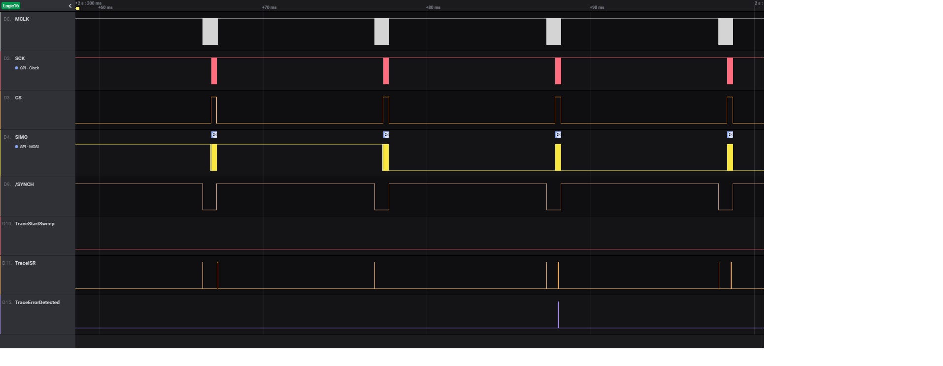
Next picture (PICTURE2) is a zoom of same capture with timing markers in the capture region where I want to focus.
Timing markers 0 (red) and 1 (green) measure the 5us delay from SPI RX trigger to DMA transfer.
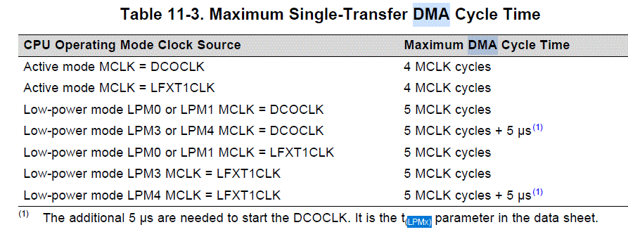
This 5us delay I understand is the one described in MSP430FR59xx User´s Guide (SLAU367P) section "11.2.7 DMA Transfer Cycle Time", to turn on and sincronize with DCO.

PICTURE2: https://drive.google.com/file/d/1qc81qf2zQKgUprw3TGEE1_1P66BQA4Rj/view?usp=sharing

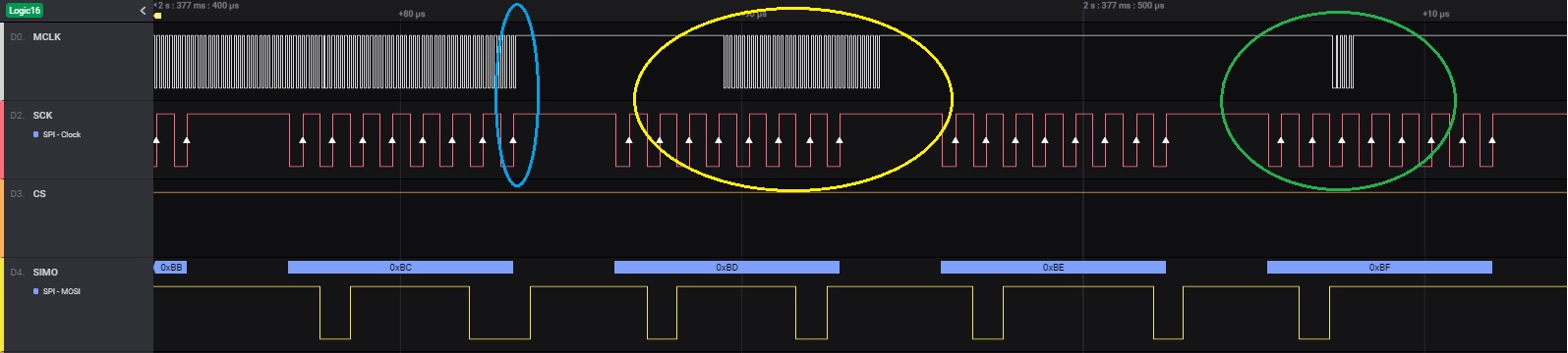
The problem I´m having occurs when main routine returns to LPM3 just when the SPI RX trigger occurs (8th SPI clock) as ilustrated in next picture (PICTURE3, larger zoom of PICTURE2).

PICTURE3: https://drive.google.com/file/d/1YpIOWE4wpv1D9PGfRybSAZWmq4q9fduA/view?usp=sharing

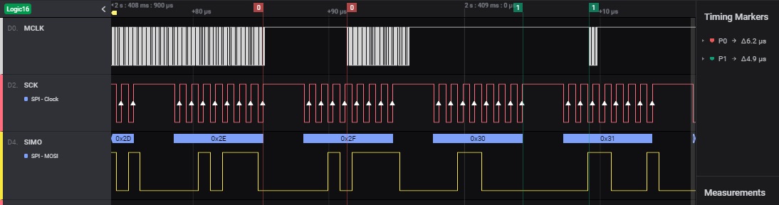
The MCLK signal becomes active for approx. 5us or 6us (timing marker 3, orange) for DMA transfer of 2 received bytes (the pending 0x9A byte and the just arrived 0x9B byte), while a single byte transfer takes 0.625us (see timing marker 2, purple).
The problem is that many times this scenario is observed, inspecting the RAM buffer (DMA destination), the 2 bytes transfered bytes by DMA, have the value of the latter one, 0x9B in this case.
The processing of the RAM buffer (destination of DMA), confirms that the position for byte 0x9A has the 0x9B value, and position of byte 0x9B has 0x9B value as expected (the status message issued for this test was forced to a incremental sequence to aid in problem detection at the slave microcontroller).
As the 0x9B value is present in UCB0RXBUF by the time of the 8th SCK rising edge, I conclude that the 2 DMA transfers occur by the end of the 5us/6us burst of MCLK (timing marker 3, orange).
In some cases, when inspecting the RAM buffer, the byte sequence buffered is shifted as if it had lost the 0x9A trigger: it doesn´t contain the byte 0x9A and the 0x9B byte is not repeated, seems like the 0x9B byte trigger for DMA has overriden the 0x9A byte pending trigger.

Considering the observed scenario and that:

 - I have no other interrupts involved (I confirmed that, setting another trace signal inside all ISR´s for the rest of Interrupt Vector entries, and none of them occurring here)
 - No FRAM access is involved in these DMA transfers

Questions:

 Can the extra MCLK burst time observed in timing marker 3 (orange) be explained by any microcontroller hardware artifact ?
 Could you confirm that the 5us delay described in section 11.2.7 correspond to the one observed by timing markers 0 (red) and 1 (green) ?
 Could the errata CS7 be related with this problem ? (although the observed MCLK burst is at 8Mhz as expected)


Additional comments and information:

 - MCLK and DCO are configured at 8Mhz ( CSCTL1 = DCORSEL | DCOFSEL_3; ) and SMCLK is configured on with a divider of 2 (4Mhz).
 - I configure DMACTL4.DMARMWDIS bit in 1, but the problem is also observed setting it to 0.

  • Picture 2 looks like an Rx overrun, which matches with your other symptoms. By simple (bad) luck,  Rx byte (N) completed just as MCLK shut down, and by the time it started up again Rx byte (N+1) had already completed. That first MCLK burst does look rather long, but I'm not sure it's outside the spec.

    On the Tx side, the SPI has 2 bytes of buffering (TXBUF+shift register). On the Rx side it only has 1.875 bytes of buffering, since when the final bit is shifted in the byte is immediately forwarded to the RXBUF.

    I've never looked, but I wouldn't be surprised if MCLK does a few more cycles after the CPU has "committed" to CPUOFF, so it's hard to tell exactly when the LPM3 started (was requested).

    SPI has no flow control, so the slave is subject to the whims (timing) of the master. The two obvious solutions/workarounds would be (1) LPM0 (<1us startup) (2) introduce an artificial delay between bytes in the master. 

  • A slower SPI clock would do the trick too.

    The overrun error flag is kind of useless when using DMA. It would be nice if it could trigger an interrupt.

  • The problem was not observed if LPM0 is used instead of LPM3. Unfortunately, due to consumption restrictions for the designed device, it has to sleep in LPM3.
    At the moment, the only feasible workarounds are to reduce SPI clock or increase the gap time between bytes, both at the master side, and avoid SPI RX overrun if the delay occurs.
    The concern is that as you don´t know the root cause of the delay, you can´t assert that it will always last the same. I am discussing with my design team to increase the byte gap at master side in 6us or 8us which seems feasible, but not in larger time (>20us) just to be protected against unknown variations of such delay.

    We have stripped the code of master and slave to the minimum and still be able to reproduce the problem causing the race condition between going to LPM3 and SPI RX.
    We have reached a strange finding on this problem:
     - a nop sequence "tunning" (between 0 to 3 nops) could be needed before entering in the slave loop, to help the problem to occur.
     - once "tuned", adding any extra sequence in that point, of a multiple of 4 nops, keeps the problem happenning, any other amount of nops makes the problem to disappear.
     
    It is C code built in a IAR (7.11.1) workspace, which performs the following:
     Master:
      - Initialize peripherals
      while ( true ) {
       - Activate /SYNCH signal (not present in real design, used here just to let the slave synchronize and go to LPM3 in a moment such to trigger the problem)
       - Wait 500us
       - Send a status packet through SPI (status data was forced to be an increasing number sequence to let slave know the expected values)
      }
     Slave:
      - Initialize peripherals
      - Nop sequence (0 to 3 nops) to cause some strange code alignation that helps the problem to occur.
      - Prepare DMA for reading SPI RXBUF (with size of packet) and enable DMA interrupt
      while ( true ) {
       - Sleep in LPM3 until interrupt of /SYNCH signal to synchronize with master duty cycle.
       - Execute nops for approx. 650us and go to LPM3 (a variation from 1 to 16 nops is included to sweep around the moment of the race condition)
       > The ISR for DMA processes the buffered data and prepares DMA again.
      }
      
      
    I am attaching here the sample source code as IAR workspace zipped and some logic signals captured with Logic2 software v2.2.18 (ideas.saleae.com/.../).

    TestDMA_20200807.zip

    Signal Capture 20200807.zip

    Both microcontrollers used are MSP430FR5989EP and connections between them and trace signals are described in connections.txt
      Master                                     Slave
      Pin #            Signal                    Pin #
      2                ----- SCK    ---->        2
      3                ----- CS     ---->        3
      4                ----- SIMO   ---->        4
      5                <---- SOMI   -----        5
      39               ----- /SYNCH ---->        39
      .                TraceErrorDetected        32
      .                TraceStartSweep           10
      .                TraceISR                  11
      (Pin numbers refering to MSP430FR5989 RGC(VQFN))
      
    Some unused ports of the microcontrollers in this sample are defined as analog or digital inputs because it was used on specific board designed, and also some internal resistors are configured.

    In this sample code, the SPI clock frequency was changed to 1.143 MHz, because working at 1 MHz was very frequent to observe in captures that the delay was present, but the DMA may have been performed just before the arrival of 8th bit of the following byte because the data error in buffer was not produced.
    Some trace signals were defined in slave microcontroller to trigger the capture in the logic analyzer and identify a failing scenario.
    Also a trace was added to each ISR routine to confirm that the delay does not correspond to an interrupt delaying DMA, something already supposed but not explicitly confirmed up to the moment.
    With this SPI frequency change, the problem presents most of the times as an overrun condition and a received byte is lost, so DMA transfer finishes when receiving first byte of the following packet, then triggers the processing of buffer and the error is detected.
    So, when the TraceErrorDetected signal makes a pulse during a packet reception, the delay and race condition most probably occured in the previous packet transmission.

    Focusing on the strange nop sequence (0 to 3) required to be adjusted to trigger the problem, we have found that when making minor changes in the code (like removing routines not used, or adding traces and adjusting execution to make coincide an SPI 8bit arrival with entering to LPM3) and the problem disappeared, we just only had to adjust again the amount of nops (0 to 3) of this sequence to make it happenning again.
    We thought that such changes could be causing to missalign/realign code to favor or not a FRAM cache miss in such point, however the DMA transfer would not require FRAM because source and destination are RAM.
    We tried changing NWAITS from 0 to 1 and adjusting nops sequences to make the delay appearing, but the delay length is the same than when having NWAITS in 0, so it doesn't seem to have FRAM access involved.

    I hope someone on TI can reproduce this problem and better understand what causes this delay, not only to design a correct workaround on our current proyect, also to allow considering this issue in future proyect designs in which we expect to use FR59xx family microcontrollers.

  • Hi Juan

    Sorry for the late response. 

    Just one more questions here that the error just happen at time to send the 0x9A?

    I saw your test code is a little complicated could you make it more simple and less code that will be cost less time to reproduce your problem. Thanks.

    Best regards

    Gary

  • Hi

    I have set up a hardware that use MSP430FR6989(Same family with MSP430FR5989) to running your code. But the wave look different with yours.

    https://e2e.ti.com/cfs-file/__key/communityserver-discussions-components-files/166/8-MHz_2C00_-200-M-Samples-_5B00_3_5D00_.logicdata

    For the test code I just make changes as below:

    1. Change the device to MSP430FR6989

    2. Comments the IAR version error "#error Expected compiler version 7.11.1"

    3. Add code of "

    P5DIR |= BIT0;
    P5SEL1 |= BIT0; // Output MCLK
    P5SEL0 |= BIT0;

    " to ouput MCLK in slave device

    Here are some questions from my side

    1.No signal on SOMI dose it right?

    2. No signal on syn signal does it P1.0 right?

    3. I saw all first data send after the CS is high is always 0xFA, does it right?

    By the way, an important reason the I want you to provide a simple example like just use DMA and SPI peripheral is that it can exclude the effect of other code. 

    Best regards

    Gary

  • Hi Gary,

    Thanks for reaching to setup a similar hardware to attempt to reproduce the problem.

    Observing your captured data, I see MCLK is at 2Mhz, please configure it to 8Mhz (and keep NWAITS at 0) to let the CPU entering LPM3 while the SPI bytes are arriving. (My InitClocks routine sets DCO and MCLK at 8Mhz).

    Below are answers to your questions:

    1.No signal on SOMI dose it right?

    Yes, it is right. It is not relevant for this scenario. And having SOMI always at 0 is due to writing 0 to SPIuC_UCxxTXBUF in PrepareDmaReading routine.

    2. No signal on syn signal does it P1.0 right?

    This signal is expected output from master and expected input on slave at P1.0 with interrupt enabled. The signal output should be always at 1 on master, and go to 0 to let Slave synchronize and trigger the dummy execution and entering LPM3 while SPI clocks are arriving.

    3. I saw all first data send after the CS is high is always 0xFA, does it right?

    Yes, first byte is always 0xFA. Second byte is a sequence value (1 more than same byte of previous sequence). Third byte is same value as the second byte. And for the following bytes the value is an increment of 1 of previous byte, eg: 0xFA, 0x5E, 0x5E, 0x5F, 0x60, 0x61 ... It is just a simplification of the real message exchanged in our development, with the addition of sequentiallity to allow this error detection at slave microcontroller.

    The provided code was already a big simplification of my custom development, but keeping all the hardware configuration used in the slave to let you know the conditions in which it is happenning. I probably may can reduce the source code a bit more eliminating ports definitions and ISR routines for interrupts not expected to occur. However, the point where I want to focus is in the race condition between the LPM3 entrance and the arrival of an SPI Rx interrupt, and its impact on the trigger of a DMA module connected to such SPI port. It seems that something in hardware is also triggered that requires CPU with higher priority than DMA.

    Best regards,

    Juan Andres

  • Hi Juan

    The reason of the MCLK is 2MHz is that I use wrong sample rate of 8Mhz with the Saleae. When I set it to 50MHz the MCLK is 8MHz.

    https://e2e.ti.com/cfs-file/__key/communityserver-discussions-components-files/166/50-MHz_2C00_-200-M-Samples-_5B00_2_5D00_.logicdata

    Now I can get the waves like yours but I don't find any problem waves. Could you show me how to modify the code to reproduce the issue?

  • Hi Gary,

    You are very close to reproduce it, we now need to help synchronize events as ilustrated by the yellow arrow:

    We have to add a 4us delay approx. in slave microcontroller before the swtich that implements a sweep. If you look at source code, it could be added by changing DelayUs(650) to DelayUs(654), or by introducing nops (approx. 32 nops) in the already present nops sequence:

      // Dummy execution from NotSYNCH signal to overlap with SPI communication
      DelayUs( 650 );

    // Placing nops here to help the race condition which triggers the problem (*) to occur in about the middle of the sweep.
    // If any change in code or ISRs is done, the dummy execution duration may vary, so tunning may be required.
    // (*): Entering to LPM3 while the 8th bit of a SPI byte has arrived and triggers DMA.
      nop10(); nop10(); nop10();
      nop(); nop(); nop(); nop(); nop(); nop(); nop(); nop(); nop(); nop(); nop();

    I measured that 4us would be needed to let the middle case of the sweep to align with the 8th bit (as indicated by yellow arrow in previous picture).

    You can add to the analizer the TraceStartSweep signal at P5.0 of slave. It is a simple pulse indicating the cycle running the first case of the sweep. So you can tune the alignment to occur for a test cycle in middle of 2 pulses of this trace, and this is where the problem would most probably be observed.

    Another useful trace signal is TraceErrorDetected (P2.1) which marks that the problem occured and a byte transmission was lost by DMA. This trace shall appear in a cycle where the byte loss is detected, but the byte loss ocurred in previous cycle:

    If the problem occurs, the DMA losses a byte transfer, and it doesn't complete the configured transfer size until reception of first byte of the following test cycle. This is also observed in the TraceISR pattern (P5.1) because DMA ISR doesn't occur in the cycle where problem occurs:

    So, you can assist with TraceErrorDetected signal (P2.1) to check if you reached the problem conditions.

    Once the entrance to LPM3 and 8th SPI clock are aligned, it may still not be enough to be in the conditions which trigger the problem. If TraceErrorDetected signal pulse is not observed, you probably have to add 1, 2 or 3 nops (or (un)comment the nops already placed in code after calling InitPeipherals routine, highlighted here in green):

    void main( void )
    {
     InitPeripherals();

    // Place between 0 to 3 nops to get the condition which triggers the problem (comment/uncomment any of the following 3 nops)
     nop();
     nop();
    // nop();

    // Once tuned, addind here a multiple of 4 nops keeps the condition to occur. Other amount of nops may cause the condition to disappear.
     nop();
     nop();
     nop();
     nop();

    In the cycle where the problem occurs, you would see a MCLK pattern like the yellow elipse in next picutre, instead of the expected MCLK pattern for DMA activity as in the green elipse. (0xBE byte is transfered at DMA activity in green elipse, 0xBD is transfered at the end of MCLK burst of yellow elipse, and 0xBC byte is lost by DMA due to the unexpected delay and overriden by 0xBD byte arrival).

    The cyan elipse is zoomed in next picture to illustrate the particular algnation observed where this problem occurs.

    Every time I observe the problem, the algnation beween MCLK and the 8th SPI clock is observed like this:

    Hope these indications are accurate for the 2 remaining fine adjustments you need in your setup to observe the problem.

    Please let me know if you reach or not the problem conditions.

    Best Regards,

    Juan Andres.

  • Hi Juan

    It seems I have reproduce the phenomenon as you seen 

    https://e2e.ti.com/cfs-file/__key/communityserver-discussions-components-files/166/40-MHz_2C00_-200-M-Samples-_5B00_10_5D00_.logicdata

    I have a question here where you configure the #define DefaultP1IE     ( 0x00 ) the means you have not enable the P1.0 interrupt. Where you configure it, I can't find it in your code.

  • Hi Gary,

    It is great news you could reach to reproduce it.

    The P1.0 interrupt is enabled at the begining of the slave main loop (see line highlighted in green):

     while ( true ) {

      // Sleep until NotSYNCH signal goes to 0 and interrupts
      P1IE_bit.NotSYNCH = true;
      __low_power_mode_3();
      __no_operation();
      P1IE_bit.NotSYNCH = false;
      P1IFG_bit.NotSYNCH = false;

      ...

    After interrupt is serviced (by routine __ISR( PORT1 )), it is left disabled to be sure the unexpected CPU delay observed was not related with an interrupt.

    The falling edge selection is configured in DefaultP1IES and applied to P1IES in InitPorts routine.

    Best Regards,

    Juan Andres

  • Hi Juan

    Thank you for your explain . 

    I have put some delay between two bytes send in the host project by the code below

    for ( UINT8 i = 0; i < n; ++i ) {
    PutTxBufAndReadRxBuf( *d );
    ++d;
    __delay_cycles(30);// add it by Gary Gao
    }

    This just add about 4 us between two bytes send(13.5us total) and the issue seems not happened again 

    https://e2e.ti.com/cfs-file/__key/communityserver-discussions-components-files/166/40-MHz_2C00_-200-M-Samples-_5B00_17_5D00_.logicdata

    It is not in larger time (>20us) have you test the workaround before? 

  • Yes,

    As an emergency workaround, I have already requested to add in master microcontroller a delay between bytes, because we are deliverying protoptype units to the customer and the problem caused by this issue has presented many times. I proposed the addition of 8us to be far enough according to the observed cases.

    My concern is that I need to assert that such a delay is safe for any case, and if we don't understand what is the cause, we can't grant it will always behave in this way, maybe it varies across parts, or changes in temperature or voltage, maybe it is related to certain configuration used or to an errata already identified but with different symptoms. Do you follow me?

    Best Regards,

    Juan Andres

  • Hi Juan

    I think the most likely reason is that the wake up time from LPM3 to active. You know the DMA is using the MCLK that is the active mode with CPU off.

    That means the time interval should large than 10us. You can see your problem waves the time interval is about 8.8us that is not enough for MSP430 to wakeup form LPM3

    Best regards

    Gary

  • Hi Gary,

    I have already considered that information from slas789d and also the note (1):

    Datasheet

    And here the identified delay is having MCLK already oscillating. The wakeup time you refer I understand is the one between the 8th SPI clock event and the MCLK start oscillating as tagged with P0 and P1 markers in following picture:

    Such delay seems be predominated by FRAM activation time during wakeup, which it is stated as included in ( t WAKE-UP LPM3 ).

    Is note (1) incorrect?

    Best Regards,

    Juan Andres

  • Hi Juan

    I have also find some parameters in the user's guide

    That seems we just need about 5 us to wait the MCLK setup. 

    But it seems more likely that this issue happen when the CPU going into LPM3 at the same time a DMA request appearing. For the picture you send above you will miss the byte "0x2F" right?

    Best regards

    Gary

  • Hi Gary,

    I disagree, I think the 5 us mentioned in Table 11-3 (slau367) are those seen before MCLK starts oscillating, like the interval tagged by P1 markers in the last picture posted, from the trigger event to the time MCLK is ready.

    Then as stated in section 11.2.7 (slau367) it takes 5 MCLK cycles to complete synchonization and transfer. Those 5 cycles are observed in the logic analyzer captures when DMA transfers occur during LPM3 intervals.

    By the way, I didn't find any symbol starting with tLPM in datasheet slas789, does this reference intend to point to tWAKE-UP LPMx ?  If that is the referenced symbol, such time occurs before the MCLK starts oscillating as explained by note (1) (slas789, Table 5-9, page copied in previous post).

    In the picture of previous post, the missed byte is 0x2E. When byte 0x2F is arriving, the DMA transfer of 0x2E is still pending. The extra MCLK cycles observed delay such transfer so much that 8th bit reception of byte 0x2F occurs first, overrides the RX flag, and when DMA finally takes place it only process a single flag, and transfers the contents of RXBUF: 0x2F. Hence, byte 0x2E was missed.

    Also, do you have any idea about the execution alignation caused by the 0 to 3 nops added at the begining of main to force the problem disappear or reapper depending the amount of nops, and that once the problem is present it persists if adding only a multiple of 4 nops?

     Best regards,

    Juan Andres.

  • Hi Juan

    I will discuss with our team first about this issue, and feed back to you later.

    This is the test code I do with MSP430FR6989

    TestDMA_20200915.zip

  • Hi Juan

    After discuss with our team we have found the root cause here:

    1. The code is using the PMM29 workaround of delayed FRAM wake-up to prevent PMM29 ERRATA à clearing FRLPMPWR in GCCTL0
    à with this the wake-up time is extended to twakeLPM3 + twakeFRAM which means 10us max + 10 us max means 20us

    2. Due to the PMM29 workaround the wake-up takes longer because FRAM LDO needs to be started now à therefore we have the additional MCLK cycles because Core LDO is up but Core not released because waiting on FRAM LDO.

    3. Due to the extended wait time of max 20us (~13us typical) the next SPI byte already received (within 10us) and therefore the RXBUFFER is filled with new data before the old one can be transferred by DMA.

    Best regards

    Gary

  • Hi Gary,

    So, do we have to consider a max of 20us (~13us typical) wake-up time even when DMA transfer does not involve FRAM as source address?

    I thought FRAM would not be required to be powered up for DMA transfer as source and destination where RAM addresses. And that FRAM would be powered up when wakeup cause was an ISR execution.

    Regarding your observation (t wake-up workaround) and my understanting that FRAM is not required for DMA in this case, it seems like the RX IFG arrival just when entering LPM3, is causing a FRAM power up in the following wake up for DMA. Therefore, the normal DMA delay from RX IFG while device is in LPM3 is  ~7 us typical (t wake-up LPM3) and if this unexpected FRAM power up occurs, then the delay increases to ~13 us typical ( + t wake-up FRAM), as observed in the captures.

    I will take the 20us time as worst case of wake-up for the workaround of adding a delay between bytes in master microcontroller.

    Best Regards,

    Juan Andres.

  • Hi Juan,

    correct, please consider 20us worst case wake-up time between the data transfers.

    And correct depending when the RX IFG arrival happens it can be that the first DMA transfer triggers FRAM wake-up. This is because we accept RX IFG DMA triggers all the time but the has different ways to handle it depending when the DMA trigger happens. However functional wise everything is as expected.

**Attention** This is a public forum