This thread has been locked.

If you have a related question, please click the "Ask a related question" button in the top right corner. The newly created question will be automatically linked to this question.

MSP430F5437A: GPIOs selection bit for I/O and Secondary purpose

Part Number: MSP430F5437A


Hi,

we are using MSP430F5437A for one of project. During initialization we made gpio port 8 as I/O and direction output. Is there any possibility for that port forcefully change that port selection to secondary purpose(TA0 timer interrupt registers) in the middle of program running and without involvement  of program.

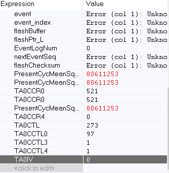
During TimerA0 initialization we made below configurations and stored 521 to TA0CCR0 register for ADC sampling purpose

Init timer1-A0 control registers for ADC sampling timer
*/
TA0CTL|= TASSEL_1; /* Clock Source: ACLK */
TA0CTL|= MC_1; /* Up mode */
TA0CTL|= TACLR; /* CLear timer counter */
/*
Init sampling timer period
*/
TA0CCR0= 521
/*
Enable timer Output mode set/reset
*/
TA0CCTL0|= OUTMOD_3; /* Out mode */


During debugging of code, we observed, apart from TA0CCTL0 all other control registers(TA0CCTL1 to TA0CCTL6) set to '1' once ADC interrupt service routine triggered in the code. This indicates capture/compare interrupt is pending, as per the data sheet. Is it expected those control registers set to 1 or it should not happen as in the code we didn't use those control registers in the initialisation.

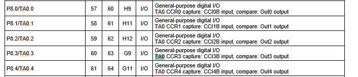
Could you please let me know what is the exact meaning for P8.0/TA0.0 in the below table.

Below table is for your information.

Thanks,

Gourav

  • Hi,

    Attached snaps for more information.

    Thanks,

    Gourav

  • 1) No, the PSEL registers will not change on their own.

    2) The TimerA CCTL registers contain a mixture of control and status bits. The status bits can/will change on their own. More generally, IFG bits in the MSP430 are set independently of their respective IE bits. It is routine to see IFGs set for events you aren't interested in.

    3) P8.0/TA0.0 denotes the GPIO function and the alternate function for the pin, similar to the pin diagrams [Figure 4-1 ff]. Perhaps more useful is Table 6-54, which shows how to configure the pin for each function.

  • Thanks Bruce for your quick response.

    Actually we used P8.0 and P8.4 as I/0 and output direction. Some times we were able to see active high pulse on those pin even pretty sure that we are not trying to set those pins to high. So we have a doubt on alternate function overlap.

    As we are using TA0CCR0 for ADC sampling timer in the code, will it impact on P8.0/TA0? 

    In Capture/Compare mode of TimerA0 of up mode, once timer count reaches TA0CCR0 how this action will inform to ADC to start sampling, by using Out[0-6] signal? 

    Figure 1-1 in 

    Thanks,

    Gopinath


  • 1) At reset P8OUT is Undefined [Ref User Guide (SLAU208Q) Table 12-2, so if you don't explicitly set P8OUT you'll see whatever is there.

    2) If you don't connect P8.0 to TA0 (using P8SEL) its activity won't be visible on the pin.

    3) You request for TA0.0 to trigger the ADC by setting ADC12SHS=1 [Ref Data Sheet (SLAS655F) Table 6-8]. TA0.0 does not need to be connected to the pin in order for this to work.

    The ADC looks for a PWM-ish waveform coming from the timer [Ref User Guide Fig 28-4/5]. With SHP=1 (Fig 28-5; recommended) it only looks for a rising edge. To generate this waveform, set OUTMOD=4 (Toggle) since none of the other OUTMODs really work for CCR0. 

    [Edit: Fixed clumsy sentence.]

**Attention** This is a public forum