This thread has been locked.

If you have a related question, please click the "Ask a related question" button in the top right corner. The newly created question will be automatically linked to this question.

MSP430FR2353: Design questions

Part Number: MSP430FR2353
Other Parts Discussed in Thread: MSP-EXP430FR2355, MSP430FR5994

Dear *,

we wan to use MSP430FR2353 for our project and have couple of questions regrading ADC and DAC

1) DAC

Can we use SAC0 OA in voltage follower configuration ( buffer) for DAC SAC0 and how?
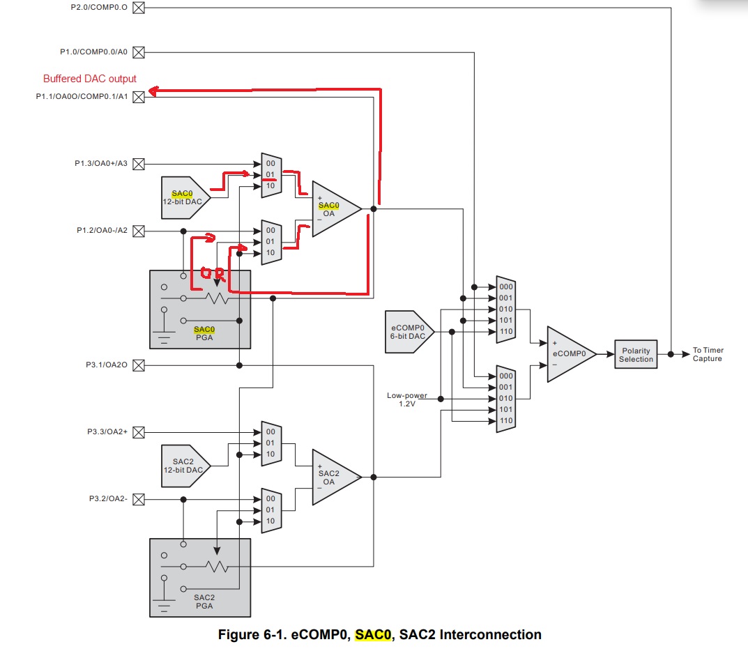
2) Does the SAC0 DAC module or SAC0 OA module have output enable register?

3) ADC

Can we use MSP430FR2353 ADC in 10 bit mode ?

we will use three analog inputs to measure three different values.

a)The questions is how many values can we measure in 10us ?

b)

If we use 10bit ADC with 6MHz

tsample = 0.52us

tsettling = 0.1us

tconversion = 2us

so for one sample and conversion we have 2.62us is that correct?

c)

no we switch to second input and again do the conversion, does the second conversion also needs tsettling?

d)

Is there also time between the two conversion ( when the input ADC switch goes from one analog pin to other)  that needs to be calculated into equation ?

Best Regards,

David.

  • 1) I suspect the answer is Yes, but I really should leave this to the EEs.

    2) No. Once you turn on DACEN/OAEN, the output goes right to the pin [Ref Data Sheet (SLASEC4C) Fig 6-3 + observed behavior]. The PSEL=0b11 setting only serves to turn off the Schmitt trigger, so it doesn't get in the way.

    3) Yes. Set ADCRES=1.

    b) I'm not completely sure where they got 0.52us from in DS Table 5-21, since my calculator says 4/6MHz=0.66us, but the difference is negligible. Assuming SHT=0, I get (4+12+1)/6MHz=2.8usec which is about what you got.

    c) You probably shouldn't get bogged down by Tsettle=0.1us, since that's about half an ADC clock, i.e. you probably can't measure it. As a practical matter, there is no settling time.

    d) See also (c). You do need to account for the time it takes to switch the channel in the ADC, which you probably can't do in less than about 15 CPU clocks.

    More generally, you need to account for:

    A) The (CPU) time to start the ADC,  figure out that it's finished, and  fetch the result.

    B) Any extra (S/H) time you need if your input isn't very low impedance.

  • Hi,

    Thank you for replay Bruce.

    1) I think the SAC OA can be used as buffer for SAC DAC ( SLAA833A page 11) E2E team please confirm

    2a) I think i can use OAEN bit 8 from SACxOA register , when '0' output on pin high impedance, when '1' output on pin is from OA

    Can you tell what is the delay when switching OAEN bit 8 from 0->1 and 1->0 ?

    2b) Or i can connect GND on OAx+ pin and then switch PSEL port between '00' and '01'

    Can you tell what is the delay when switching PSEL bit 0-1 from 00->01 and 01->00?

    3a)The questions is how many values can we measure in 10us ?

    3b) They got the 0.52us from the following formula tsample = ln(2^(n+1)) × τ where τ = (Ri +Rs)*(Ci+Cex)

    Rs = External source resistance

    Ri = Internal MUX-on input resistance

    Ci = Input capacitance

    Cex = External capacitance

    Why does your calculator say 4/6MHz for tsample , where did you get the formula?

    3c/d) how do you know that it needs 15 CPU clk-s to switch from one input to other ? is this specified in DS?

    So for 24MHz -> 625ns?

    4) what is the time needed for CPU to start the ADC?

    Will the CPU give interrupt when the conversion is finished?

    Br,

    David.

  • 2a/b) Data sheet (SLASEC4C) Table 5-25 indicates an OA settling time of 1-4.5 sec (depending on OAPM).

    3b) That's 4 ADCCLKs (SHT=0) at 6MHz (max ADC clock). You could actually make this shorter by generating your own sampling pulse (SHP=0) but the logistics might be tricky. 

    3c) I wrote the code in my head and estimated the clocks for each instruction. Maybe you can do better -- write the code and count the clocks using User Guide (SLAU445I) Chapter 4. Or, better yet, code it and measure it.

    4) UG Fig 21-6 shows that (with SHP=1) it can take up to 1 ADC clock from trigger to S/H. An interrupt will be triggered at the end if you set ADCIE0.

    More generally, I suggest you buy a Launchpad (MSP-EXP430FR2355) and try/measure all these things before you "bet your project" on them. I don't think you've described more than maybe 100 lines of code.

  • Hi David,

    d_zero said:
    1) I think the SAC OA can be used as buffer for SAC DAC ( SLAA833A page 11) E2E team please confirm

    Figure 8 of the App Note https://www.ti.com/lit/slaa833 clearly shows the usage example of the voltage follower. So, yes, you should be able to use the SAC in that configuration.

    Srinivas

  • Hi Srinivas,

    on question regarding internal voltage reference.

    1)

    If we select 1.5V internal reference for ADC can we then select 2.5V internal reference in the same time for DAC?

    2)

    What voltages can we use on external VEREF+ pin ?

    3) Regarding Pin mux

    if i use eg. RSM package 32-pin MSP430FR2353TRSM and if i want use OA3O then this pin is only available on pin25 or can be set to other pin?

    Br.

    David.

  • Hi David,

    d_zero said:
    If we select 1.5V internal reference for ADC can we then select 2.5V internal reference in the same time for DAC?

    This is not possible. Only 1 voltage value can be used for both.You can see the description in the following sections of the User's guide (https://www.ti.com/lit/pdf/slau445).: Figure 2-1. PMM Block Diagram: Only 1 Enhanced shared reference is sent out to the ADC and DAC modules. Section 2.2.8 Shared Reference Generation and Distribution also explains the same. Also, 2.3.3 PMMCTL2 Register has the description of the control bits REFVSEL that lets you specify one of the voltage values. 

    d_zero said:
    What voltages can we use on external VEREF+ pin ?

    The datasheet is not clear about the allowed VEREF+ voltage ranges but I think this should be 1.2V as it basically replaces the functionality of the internal 1.2V reference voltage.

    d_zero said:
    if i use eg. RSM package 32-pin MSP430FR2353TRSM and if i want use OA3O then this pin is only available on pin25 or can be set to other pin?

    It is only available on pin 25. This can be confirmed from the datasheet's Figure 4-4. 32-Pin RSM (VQFN) (Top View) – MSP430FR235x, or Table 4-1. Pin Attributes.

    Srinivas

  • Hi Srinivas,

    why do you think that Veref+ can only accept 1.2V ?

    I think it can be also 3.3V, because of table 4.1 page 18 in datasheet, because it says the power source for Veref+ is DVCC and we will use 3.3V for DVCC ?

    Eg. the MSP430FR5994 has this specification on page 60

    10) do you see any issue to use single ended crystal oscillator ECS-2520MV-240-BN on XIN pin ?

    Best Regards,

    David.

  • Hi David,

    VEREF+: It is not clear to me from the datasheet if it can support DVCC as a valid input. But I think you are right based on the functionality of the ADC module and the description of ADCSREFx in section 21.3.6 ADCMCTL0 Register of the User's Guide (www.ti.com/.../slau445). 

    In general, I try not to use the datasheet parameters from a different sub-family even if it gives some general guidance. The MSP430FR5994 and MSP430FR2353 are from different sub-families.

    d_zero said:
    10) do you see any issue to use single ended crystal oscillator ECS-2520MV-240-BN on XIN pin ?

    This should be possible. You will need to set the HFXTBYPASS mode. You can see section 7.1.2 External Oscillator of the datasheet for some additional explanation. 

    Srinivas

  • Dear Srinivas,

    1)

    waht is the proper termination of unused I/O pins on MSP430?

    Best Regards,
    David.

  • Hi David,

    In general, the unused I/O pins can be left open. Their reset state is an OFF mode. You can see the footnote of Table 4-1 Pin Attributes of the datasheet for an explanation. 

    Srinivas

**Attention** This is a public forum