This thread has been locked.

If you have a related question, please click the "Ask a related question" button in the top right corner. The newly created question will be automatically linked to this question.

MSP432P401R: Setting up I2C with PCA9685

Part Number: MSP432P401R

Hello,

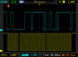
As a part of my senior design project, I am trying to drive an I2C PWM LED Driver (PCA9685 from NXP Sem, DataSheet attached). To test I understand the I2C protocol, I am just trying to turn on 1 LED channel by writing a value to a control register and reading that value back. PCA9685.pdf

Here is my code. 

/* --COPYRIGHT--,BSD
 * Copyright (c) 2017, Texas Instruments Incorporated
 * All rights reserved.
 *
 * Redistribution and use in source and binary forms, with or without
 * modification, are permitted provided that the following conditions
 * are met:
 *
 * *  Redistributions of source code must retain the above copyright
 *    notice, this list of conditions and the following disclaimer.
 *
 * *  Redistributions in binary form must reproduce the above copyright
 *    notice, this list of conditions and the following disclaimer in the
 *    documentation and/or other materials provided with the distribution.
 *
 * *  Neither the name of Texas Instruments Incorporated nor the names of
 *    its contributors may be used to endorse or promote products derived
 *    from this software without specific prior written permission.
 *
 * THIS SOFTWARE IS PROVIDED BY THE COPYRIGHT HOLDERS AND CONTRIBUTORS "AS IS"
 * AND ANY EXPRESS OR IMPLIED WARRANTIES, INCLUDING, BUT NOT LIMITED TO,
 * THE IMPLIED WARRANTIES OF MERCHANTABILITY AND FITNESS FOR A PARTICULAR
 * PURPOSE ARE DISCLAIMED. IN NO EVENT SHALL THE COPYRIGHT OWNER OR
 * CONTRIBUTORS BE LIABLE FOR ANY DIRECT, INDIRECT, INCIDENTAL, SPECIAL,
 * EXEMPLARY, OR CONSEQUENTIAL DAMAGES (INCLUDING, BUT NOT LIMITED TO,
 * PROCUREMENT OF SUBSTITUTE GOODS OR SERVICES; LOSS OF USE, DATA, OR PROFITS;
 * OR BUSINESS INTERRUPTION) HOWEVER CAUSED AND ON ANY THEORY OF LIABILITY,
 * WHETHER IN CONTRACT, STRICT LIABILITY, OR TORT (INCLUDING NEGLIGENCE OR
 * OTHERWISE) ARISING IN ANY WAY OUT OF THE USE OF THIS SOFTWARE,
 * EVEN IF ADVISED OF THE POSSIBILITY OF SUCH DAMAGE.
 * --/COPYRIGHT--*/
/******************************************************************************
 *  MSP432P4 I2C - EUSCI_B0 I2C Master TX/RX bytes to PCA9685A Slave-Repeated Start
 * 
 *  Description: This demo connects two MSP432's via the I2C bus. This is the
 *  MASTER CODE.The master transmits 2B to the slave, then receives a byte. 
 *  The master transmits two bytes to the slave followed by a
 *  repeated start and a single-byte read from the slave.
 *  This is a common operation for bytes from I2C slave devices such as EEPROMs.
 *  The transaction for the I2C that is written looks as follows:
 *  ________________________________________________________
 *  |  Start    | WData | WData | Start    | RData  |       |
 *  | 0x48 Addr | 0x007 | 0x013 |0x48 Addr |  0x13  | Stop  |
 *  |    W      |       |       |    R     |        |       |
 *  |___________|_______|_______|__________|________|_______|
 *
 *  ACLK = n/a, MCLK = HSMCLK = SMCLK = BRCLK = default DCO = ~3.0MHz
 *
 *                                /|\  /|\
 *                   PCA9685      10k  10k      MSP432P401R
 *                   slave         |    |         master
 *             -----------------   |    |   -----------------
 *            |          P27/SDA|<-|----+->|P6.4/UCB1SDA     |
 *            |                 |  |       |                 |
 *            |                 |  |       |                 |
 *            |          P26/SCL|<-+------>|P6.5/UCB1SCL     |
 *            |                 |          |             P2.7|-- Error
 *            |                 |          |             P2.6|-- Activity
 *
 *****************************************************************************/
/* DriverLib Defines */
#include <ti/devices/msp432p4xx/driverlib/driverlib.h>

/* Standard Defines */
#include <stdint.h>
#include <stdbool.h>
#include <string.h>

/* Slave Address for I2C Slave */
#define SLAVE_ADDRESS       0x48
#define NUM_OF_REC_BYTES    1

/* Variables */
const uint8_t TXData[] = {0x013,0x007};
static uint8_t RXData;

/* I2C Master Configuration Parameter */
const eUSCI_I2C_MasterConfig i2cConfig =
{
        EUSCI_B_I2C_CLOCKSOURCE_SMCLK,          // SMCLK Clock Source
        3000000,                                // SMCLK = 3MHz (default)
        EUSCI_B_I2C_SET_DATA_RATE_100KBPS,      // Desired I2C Clock of 100khz
        0,                                      // No byte counter threshold
        EUSCI_B_I2C_NO_AUTO_STOP                // No Autostop
};

int main(void)
{
    /* Disabling the Watchdog  */
    MAP_WDT_A_holdTimer();

    /* Select Port 6 for I2C - Set Pin 4, 5 to input Primary Module Function,
     *   (UCB0SIMO/UCB0SDA, UCB0SOMI/UCB0SCL).
     */
    MAP_GPIO_setAsPeripheralModuleFunctionInputPin(GPIO_PORT_P6,
            GPIO_PIN5 + GPIO_PIN4, GPIO_PRIMARY_MODULE_FUNCTION);
    MAP_GPIO_setAsOutputPin(GPIO_PORT_P2, GPIO_PIN7);
    MAP_GPIO_setOutputLowOnPin(GPIO_PORT_P2, GPIO_PIN7);

    MAP_GPIO_setAsOutputPin(GPIO_PORT_P2, GPIO_PIN6);
    MAP_GPIO_setOutputLowOnPin(GPIO_PORT_P2, GPIO_PIN6);

    /* Initializing I2C Master to SMCLK at 100khz with no autostop */
    MAP_I2C_initMaster(EUSCI_B1_BASE, &i2cConfig);

    /* Specify slave address */
    MAP_I2C_setSlaveAddress(EUSCI_B1_BASE, SLAVE_ADDRESS);

    /* Enable I2C Module to start operations */
    MAP_I2C_enableModule(EUSCI_B1_BASE);
    MAP_Interrupt_enableInterrupt(INT_EUSCIB1);

    // enable RX interrupts
    MAP_I2C_enableInterrupt(EUSCI_B1_BASE, EUSCI_B_I2C_RECEIVE_INTERRUPT1);

    while (1)
    {
	    RXData=0;

        /* Making sure the last transaction has been completely sent out */
        while (MAP_I2C_masterIsStopSent(EUSCI_B1_BASE));

        /* Send out EEPROM Mock Read Cmd (2 databytes) */
        MAP_I2C_masterSendMultiByteStart(EUSCI_B1_BASE, TXData[1]);  // Start + 1Byte
        MAP_I2C_masterSendMultiByteNext(EUSCI_B1_BASE, TXData[0]); // Poll for TXINT,Send 1Byte
        /*---------------------------------------------*/
        /* Now we need to initiate the read */
        /* Wait until 2nd Byte has been output to shift register */
        while(!(EUSCI_B1->IFG & EUSCI_B_IFG_TXIFG0));

        // Send the restart condition, read one byte, send the stop condition right away
        EUSCI_B1->CTLW0 &= ~(EUSCI_B_CTLW0_TR);
        EUSCI_B1->CTLW0 |= EUSCI_B_CTLW0_TXSTT;
        while(MAP_I2C_masterIsStartSent(EUSCI_B1_BASE));
        EUSCI_B1->CTLW0 |= EUSCI_B_CTLW0_TXSTP;
        //while(!(EUSCI_B1->IFG & EUSCI_B_IFG_RXIFG0));
        //RXData = EUSCI_B0->RXBUF;

        //---------------------------------
        //MAP_PCM_gotoLPM0InterruptSafe();

        // Slave should send a single 0x13 back
        if(RXData != 0x13){
            // Error- set P2.7 high
            MAP_GPIO_setOutputHighOnPin(GPIO_PORT_P2, GPIO_PIN7);
            while(1);
        }
        __delay_cycles(300000); // ~100ms pause between transmissions
    }
}

/*******************************************************************************
 * eUSCIB0 ISR. The repeated start and transmit/receive operations happen
 * within this ISR.
 *******************************************************************************/
void EUSCIB0_IRQHandler(void)
{
    uint_fast16_t status;

    status = MAP_I2C_getEnabledInterruptStatus(EUSCI_B1_BASE);

    /* Receives bytes into the receive buffer. If we have received all bytes,
     * send a STOP condition */
    if (status & EUSCI_B_I2C_RECEIVE_INTERRUPT1)
    {
        // One-byte Read
        RXData = MAP_I2C_masterReceiveSingle(EUSCI_B1_BASE);
        MAP_GPIO_toggleOutputOnPin(GPIO_PORT_P2, GPIO_PIN6);
    }
}

I am trying to troubleshoot by probing the interface signals with an oscilloscope, but I am unable to confirm my read or write.

Thanks so much.

  • Hi 

    I think you can follow the bus transactions of PCA9685 with the I2C. If you have any problem to use the I2C with MSP432 you can ask me here

  • >    MAP_I2C_enableInterrupt(EUSCI_B1_BASE, EUSCI_B_I2C_RECEIVE_INTERRUPT1);

        if (status & EUSCI_B_I2C_RECEIVE_INTERRUPT1)

    I think you want "EUSCI_B_I2C_RECEIVE_INTERRUPT0" here. IFG1-3 are only for Slave (multi-address) mode.

  • I have made the changes you suggested, but I am still having issues. 

    I have figured out that my program gets stuck @ 

    while(MAP_I2C_masterIsStartSent(EUSCI_B1_BASE));

    I am trying to use the Protocol Analyzer on my Digilent Analog Discovery Board 2, and I'm receiving 

    Error
    Start, h00 [ h00 | WR ],

    I also uncommented both these lines

    while(!(EUSCI_B1->IFG & EUSCI_B_IFG_RXIFG0));
    RXData = EUSCI_B0->RXBUF;

    Thanks,

  • I have also fixed a couple of mistakes in my circuit setup, do you have anymore suggestions?

  • > Start, h00 [ h00 | WR ],

    This trace looks a bit odd. It appears to be saying that it saw a slave address of 0x00, which isn't what I would expect from this code. Was there more?

    0x00 is the General Call address, which the device [Ref data sheet Sec 7.6] interprets as a Reset request.

    More generally, the SendMultiByte group doesn't check for NACK; though in that case I would expect it to hang in SendMultiByteNext.

    If you're going to poll for RXIFG, you should probably not enable the Rx Interrupt.

  • There is more now

    Error
    Start, h00 [ h00 | WR ], h00,

    This happened after I just fixed my ISR handler name, it was still trying to service EUSCI_B0.

    Now interrupts are serviced and my activity LED turns on. But, I still get errors. I have double checked my slave devices datasheet but I'm going to triple check.

  • I also tried running a similar example with no interrupts and did not receive an error but still 0x00 

  • What is still 0x00? The trace? or the RXBUF result?

    I would expect the trace to say "h48" or maybe "h90", which makes me wonder if something is mis-wired.

  • The data I'm receiving on the I2C serial data line stil reads as 0x00.

    I've quadruple checked my wiring and have fixed any errors I found. I also probed at each node to verify the VDD, VSS pins etc had the values I expected.

  • I made the changes I suggested, and fixed the ISR name, and I was able to write/read register 0x1F of an LIS3DH accelerometer attached to a Launchpad.

    There probably should be an interlock with the ISR so you don't check RXData before it runs, but it seems to (accidentally) do the right thing anyway.

    Can you describe your setup a little more? I'm guessing you don't have a Launchpad, since it doesn't have LEDs at P2.6/7. Is this a custom board?

  • I am using a Launchpad. However, a requirement of my project is to minimize simplicity associated with using a development board so I'm using external LEDs. 

    I currently have breadboard circuit setup that connects my Launchpad, my PCA9685 (it's application in design circuitry), external LEDs, external push buttons (w/ IC debouncer), and a buzzer. I've been using CCS Cloud but I have desktop installed. I've thought about using desktop to track values entering each register. However, because I am using DriverLib APIs I'm not positive what values to expect and the program flow recommend in the user's guide does not match the example. 

    I haven't found any part of the PCA manual that specifies any commands/data that must be written/read before I can write to the LED output registers.

                       		3V3 3V3   3V3
    				  | /|\  /|\
                       PCA9685        | 10k  10k      MSP432P401R
                        slave         |  |    |         master
                  -----------------   |  |    |   -----------------
          GND -->|P1/A0     P28/VDD|<-+  |    |  |                 |
          GND -->|P2/A1     P27/SDA|<----|----+->|P6.4/UCB1SDA     |       
          GND -->|P3/A2            |     |       |                 |
          3v3 -->|P4/A3     P26/SCL|<----+------>|P6.5/UCB1SCL     |
          GND -->|P5/A4  	       |             |                 |
    	     |       P25/EXTCLK|<-- GND      |             P2.7|--> Error
         Gate <--|P6/LED0	 P24/A5|<-- GND      |             P2.6|--> Activity
    	     | 		P23/OE\|<-- GND      | 		       | 
                 |                 |             |  	   P3.5|<--Switch (N/A)
          GND -->|P14/VSS	       |  	     |             P3.6|<--Switch (N/A)
     			                     |             P3.7|<--Switch (N/A)
     					     |                 |
    	   				     |        P5.7/C1.6|<--Vcompare (N/A) 		
    	   
    	  3V3
    	   |		     
    	  240
               |		             
     	RED LED				     
    	  _| D
    Gate -->||
    	||_
    	   | S
              GND

    I'll attach a txt file which contains a schematic of how my circuits are constructed. 

  • Is the PCA9685 on a commercial breakout board, or have you built something for it? One thing to check would be how the address (An) pins are wired.

    Have you figured out why the "h00" trace looks like that? If that's what's really on the bus, that would be a clue. Alternatively, can you get a scope trace?

    You might try reading e.g. register 0xFE, which I think should have the value 0x1E after startup. For now, don't try writing to it (second Tx byte), just write the register number and then do the restart.

  • Yes, the PCA9685 is on a commercial breakout board. The PCA9685 only has A5-0 but the MSP code specifies A7-A0 (0x48). I assumed hard wiring the PCA9685 to value A5 (0b001000) A0 to match the lower bits of the MSP slave address (0b0 100 1000) was the correct thing to do. I also just tried shifting the A5-0 of the PCA9685 to A6-1 of the MSP Slave address and measured "Error, Start" on my protocol analyzer. So maybe I can test some others to see if I that's what's wrong. 

    No I do not, that's why I'm asking. I'm not sure what you exactly you're referring to when you say the word "trace." Can you clarify and be more specific. I have tried setting triggers but my measuring tool does not capture the bus changes. 

    I thought of taking a different approach like that as well. I will try it now.

  • I still get the same "Error
    Start, h00 [ h00 | WR ], h00, h00, h00, h00, h00, h00, h00, h00, h00," when measuring using my protocol analyzer and my error condition is still asserted.

  • Now I'm very confused, because with breakpoints at seemingly armful places it seems errors are generated, but not when the  code just runs outside of debug mode.

  • I don't recommend trying to debug I2C in detail using breakpoints. A breakpoint doesn't stop the I2C bus, so the timing gets thrown off while you (the human) are looking.

    When I ran this code, I set a breakpoint up at the top of the while() loop, and let it run one full transaction at a time.

    The PCA9685 data sheet Fig 4 shows how the address is formed. A6 is fixed at 1 (0x40). A5-A0 depend on how your board is wired. If you've tied (only) A3=1, and the rest are tied/pulled to 0, then yes, 0x48 would be correct. (Per data sheet Sec 7.1.1, there are no internal pullups/pulldowns on the An pins, so be sure to do Something with each of them.)

  • That's  very useful advice. I will take that into account during future debug sessions. 

    I do not currently have external pullups/pulldowns, I connected the pins directly to respective power rails. I will make this change as well.

    I'll let you know how this affects what I measure.

  • I've made sure to connect my An pins to the appropriate pullup/pulldown resistors. 

    On the recommendation of my teaching assistant for the course, I am trying to understand the I2C module on the MSP432 so that I can more effectively use the DriverLib APIs to edit the code I have now to more closely follow the bus transactions examples shown in the PCA datasheet.

    I just want to be able a read the value of a specific register on the PCA to test my interface works, but there's no examples shown for that. I have posted a post on their forums pages for an example of this. 

  • I think I demonstrated that your code is capable of both reading and writing an I2C device, randomly chosen from my "gizmo box". The sequences I saw in the PCA data sheet looked fairly ordinary, so I expect your code should succeed with that. As you say, it might be useful to read up on I2C (there are plenty of Web resources) so you can better interpret the data sheet diagrams.

    But I don't have your equipment, and I can't see what you're seeing. In the absence of more diagnostics I'm not sure what else to suggest.

    If it helps any, here is a scope trace writing (0xFF), then reading back register 0x1F from an LIS3DH. The top line is SDA and the bottom SCL.

**Attention** This is a public forum