This thread has been locked.

If you have a related question, please click the "Ask a related question" button in the top right corner. The newly created question will be automatically linked to this question.

MSP-EXP430F5529LP: Using SPI with the MSP430

Part Number: MSP-EXP430F5529LP

Hi, I have an MSP430 dev board, the MSP-EXP430F5529LP.  In all of the searching I've done in this forum and elsewhere on the web it seems the "3 wire" SPI the MSP430 supports is a clock line and data in/out lines but no built-in support for a slave select line.  And that to use a slave select line you must manually toggle a GPIO output pin.  Is this really true???

  • Hi Terence,

    Yes, generally a 4th separate Slave select connect is used with 3 wire mode.

    BR,
    Leo

  • Is there no way to automate this though with the MSP430?

    Ideally, I'd like setup the SPI on the MSP430 so that all I have to do is call a transmit function with the data I wish to send and the peripheral will automatically toggle the slave select line accordingly.  This is how it's worked with other microcontrollers I've used.

    However, based on what I've read it seems this is not possible with the MSP430.  It seems I need to manually toggle a GPIO pin high/low for the slave select.  Am I correct in my understanding?

  • Hi Terence,

    Yes. Another alternative would be to use a 4 wire SPI interface.

    BR,
    Leo

  • I think user guide (SLAU208Q) Sec 37.3 is saying that with a 4-wire master the STE pin is toggled automatically. Unfortunately, I don't see an explicit statement of that in Chapter 37. (The eUSCI has the UCSTEM feature, and does say that explicitly.) 

    The reason I'm not sure is that I've never used 4-wire master on an MSP430, since the automated STE asserts STE around each byte, and every SPI slave I've worked with requires STE asserted for the entire transaction. [Ref UG Figs 37-4 and 40-4] This is not unique to the MSP430, most SPI masters work this way.

    The reason I'm speaking up: If your slave requires STE be asserted for the entire transaction, you must use 3-wire with an explicit GPIO for STE (and there's no reason to find out if it works).

  • H Bruce - Thank you for chiming in. Yes, my slave device requires STE be asserted for the entire transaction.  In referencing section 37.3, I take it you're referring to this specific quote in the datasheet:

    When reading the datasheet before posting I missed this.  I thought I'd read that the MSP-EXP430F5529LP only did USCI SPI  in 3-wire mode.

    I'll figure out how to do 4-wire master and explicitly set the GPIO for STE and post back with my results.  Thank you.

  • If you're using a GPIO for STE (/CS), you should use 3-wire mode. If you use 4-wire mode for this case you may have to wiggle the (vestigial) STE so the SPI unit sees what it wants, which is kind of a pain for no benefit. In 3-wire mode it ignores STE entirely. In 3-wire mode you can use the pin marked STE (as a GPIO) for /CS, or some other pin, whatever is convenient.

  • Bruce McKenney47378 said:

    In 3-wire mode you can use the pin marked STE (as a GPIO) for /CS, or some other pin, whatever is convenient.

    Thanks, Bruce.  This is the problem though.  My slave peripheral needs CS (chip select) and I'd prefer to not have to manually toggle a GPIO pin for the CS.  Every other microprocessor I've used before includes a CS pin with SPI that is automatically toggled before/after the data is sent, so I'm puzzled why the MSP430 does not.

    I've had some time to investigate further.  What I'm seeing in the MSP430 DriverLib doc is that it does not seem to support a chip select line :(  

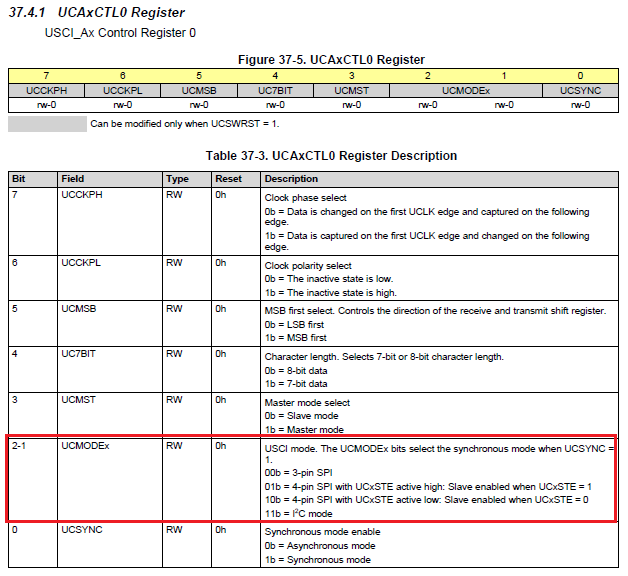
    If you look at the datasheet, you'll see it appears to support 4-pin SPI with a chip select (see register field UCMODEx below):

    If you look at the "MSP430 DriverLib for MSP430F5xx_6xx Devices User's Guide", you'll see the USCI_A_SPI_initMaster().  BUT, if you dig into the DriverLib code of this function you'll see it doesn't support modifying the UCMODE register field:

    bool USCI_A_SPI_initMaster(uint16_t baseAddress, USCI_A_SPI_initMasterParam *param)
    {
        //Disable the USCI Module
        HWREG8(baseAddress + OFS_UCAxCTL1) |= UCSWRST;
    
        //Reset OFS_UCAxCTL0 values
        HWREG8(baseAddress + OFS_UCAxCTL0) &= ~(UCCKPH + UCCKPL + UC7BIT + UCMSB +
            UCMST + UCMODE_3 + UCSYNC);
    
        //Reset OFS_UCAxCTL1 values
        HWREG8(baseAddress + OFS_UCAxCTL1) &= ~(UCSSEL_3);
    
        //Select Clock
        HWREG8(baseAddress + OFS_UCAxCTL1) |= param->selectClockSource;
    
        HWREG16(baseAddress + OFS_UCAxBRW) =
            (uint16_t)(param->clockSourceFrequency / param->desiredSpiClock);
    
        /*
         * Configure as SPI master mode.
         * Clock phase select, polarity, msb
         * UCMST = Master mode
         * UCSYNC = Synchronous mode
         * UCMODE_0 = 3-pin SPI
         */
        HWREG8(baseAddress + OFS_UCAxCTL0) |= (
            param->msbFirst +
            param->clockPhase +
            param->clockPolarity +
            UCMST +
            UCSYNC +
            UCMODE_0
            );
        //No modulation
        HWREG8(baseAddress + OFS_UCAxMCTL) = 0;
    
        return ( STATUS_SUCCESS) ;
    }

    My SPI code is shown below:

    #define SPICLK                          500000
    uint8_t transmitData = 0x00;
    
    void main (void)
    {
        //Stop watchdog timer
        WDT_A_hold(WDT_A_BASE);
    
        GPIO_setAsPeripheralModuleFunctionOutputPin(GPIO_PORT_P2, GPIO_PIN7);
        GPIO_setAsPeripheralModuleFunctionOutputPin(GPIO_PORT_P3, GPIO_PIN4);
        GPIO_setAsPeripheralModuleFunctionOutputPin(GPIO_PORT_P3, GPIO_PIN3);
        GPIO_setAsPeripheralModuleFunctionOutputPin(GPIO_PORT_P3, GPIO_PIN2);
    
        //Initialize Master
        USCI_A_SPI_initMasterParam param = {0};
        param.selectClockSource = USCI_A_SPI_CLOCKSOURCE_SMCLK;
        param.clockSourceFrequency = UCS_getSMCLK();
        param.desiredSpiClock = SPICLK;
        param.msbFirst = USCI_A_SPI_MSB_FIRST;
        param.clockPhase = USCI_A_SPI_PHASE_DATA_CHANGED_ONFIRST_CAPTURED_ON_NEXT;
        param.clockPolarity = USCI_A_SPI_CLOCKPOLARITY_INACTIVITY_LOW;
    
        returnValue = USCI_A_SPI_initMaster(USCI_A0_BASE, &param);
        if (STATUS_FAIL == returnValue){
            return;
        }
    
        //Enable USCI_A_SPI module
        USCI_A_SPI_enable(USCI_A0_BASE);
    
        //Configure port pins to reset slave
        // Wait for slave to initialize
        __delay_cycles(100);
    
        // Initialize data values
        transmitData = 0x00;
    
        //Transmit Data to slave
        while(1)
        {
            USCI_A_SPI_transmitData(USCI_A0_BASE, transmitData);
            transmitData++;
        }
    }
    

    When running my code and viewing the MSP430's pins with my logic analyzer, I see this:

    ^As expected, nothing on P3.2, the UCA0STE.  I even tried to manually set the register fields after calling USCI_A_SPI_initMaster() in hopes it'll properly activate it by doing this:

    UCA0CTL0 |= 0x1;
    UCA0CTL0 |= UCMODE_2;

    ...but that doesn't appear to work as when doing so my logic analyzer shows nothing at all, not even on the SCLK or master out lines.

    Is there maybe a different model of the MSP430 that supports this???

    Any thoughts on this would be very much appreciated.

    Thanks

  • It appears your original information was correct. As near as I can tell the USCI (as seen on the F5529) doesn't support dynamically driving of STE in any mode. With UCMODE=2 or 3, STE is an input to the Master. You have to drive the slave /CS yourself.

    I tried 4-wire mode, but I used the REN resistors to pull STE to inactive state (so the master is Active). The fact that I succeeded with this tells me that STE is an input, so you won't get it to drive the slave's /CS pin. Another clue is in UG Table 37-1: With UCMODE=2 (STE active low) making STE active (low) makes the master Inactive, i.e. if the master set STE active it would stop (contradiction).

    The eUSCI (seen in more recent MSP430 devices) supports auto-STE using UCSTEM=1. The USCI behavior seems to match the eUSCI behavior when UCSTEM=0.

    For reference, here's the program I used:

    #include <msp430.h>
    
    int main(void) {
        WDTCTL = WDTPW | WDTHOLD;
    
        P3OUT |= BIT2;          // STE
        P3REN |= BIT2;
    
        //  mode=(0,0), master, MSB first, sync, 4-pin (L), SMCLK
        UCA0CTL0 = (1*UCCKPH) | (0*UCCKPL) | UCMST | UCMSB | UCSYNC | UCMODE_2 ;
        UCA0CTL1 = UCSSEL_2 | UCSWRST;
        UCA0BRW = 2;            // 500kHz, I suppose
        UCA0CTL1 &= ~UCSWRST;
    
        P3SEL |= (BIT2 | BIT3 | BIT4);  // STE, MISO, MOSI
        P2SEL |= BIT7;                  // SCK
    
        while (1)
        {
            P3OUT |= BIT2;      // STE inactive, so master active
            UCA0TXBUF = 0x55;
            while (UCA0STAT & UCBUSY) /*EMPTY*/;
            P3OUT &= ~BIT2;
             __delay_cycles(2*2*8);       // 2 byte times at BRW=2 for the scope
        }
        /*NOTREACHED*/
        return (0);
    }
    

  • Okay, thank you Bruce for confirming.  I'll take a look at some of the MSP430's supporting eUSCI.

**Attention** This is a public forum