


Greetings,
Does TI make available a block diagram or equivalent circuit for the GPIOs on MSP430FR2676? For example, on a similar part produced by a different vendor, they provide the following diagram:
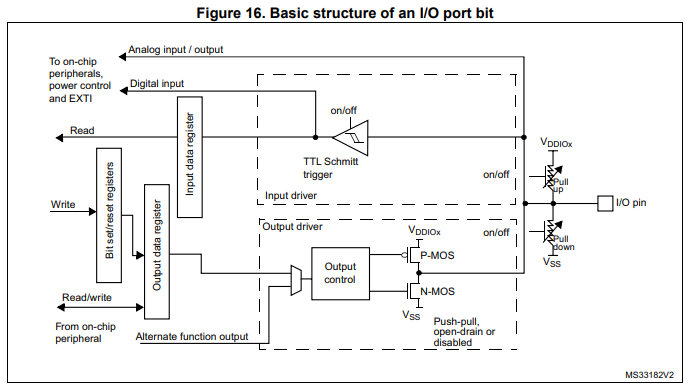
In particular, I am wondering if reading the actual driven output state of an output port is possible without connecting to another pin set up as an input. Reading the output data register will not suffice because we need the ability to verify what the actual pin state is for our application. In the above example, this is possible as the CMOS output ties directly to the input buffer, which can be enabled even if the pin is in output mode. I was able to find the following from ag_08.pdf (ti.com), which seems to be a very old document and doubt it's relevancy to newer MSP430 models:

Thank you,
Carter


