Part Number: MSP430F5529
Tool/software: Code Composer Studio
hi everyone
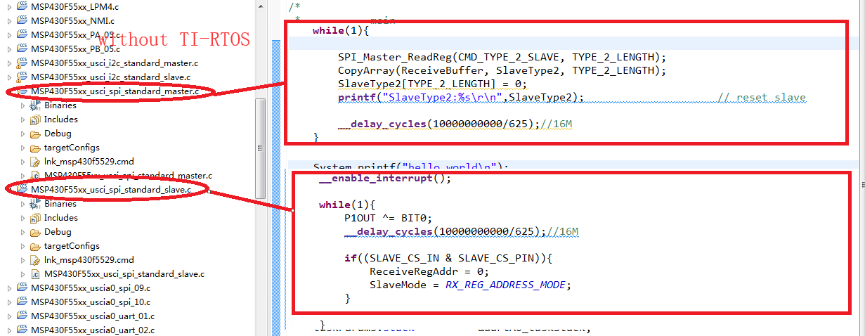
I now need two EXP_MSP430F5529LP development boards to verify SPI communications, one of the master mode (running ti-rtos), the other running SPI slave mode (without ti-rtos), and now I use the 【MSP430F55xx_usci_spi_standard_slave】 example code of SPI slave mode.
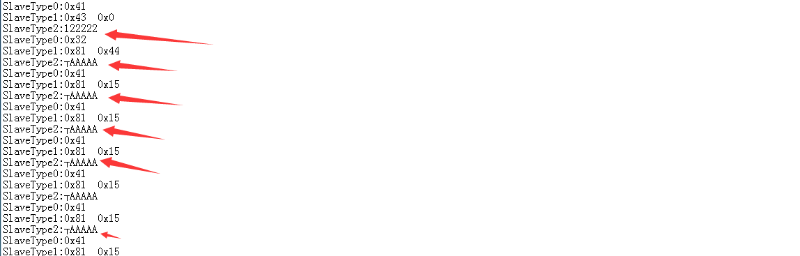
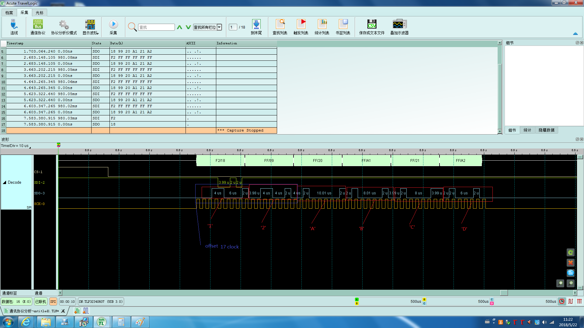
now I found that the spi master mode is only normal for the first time reading data, the rest is failing, you have to reset the slave mode development board once to read the normal data.I don't know why? Now just want to simulate the slave module board as spi flash, who has better advice?
thank you
xc_mo
MSP430F55xx_usci_spi_standard_slave code
//******************************************************************************
//   MSP430F552x Demo - USCI_A0, SPI 3-Wire Slave multiple byte RX/TX
//
//   Description: SPI master communicates to SPI slave sending and receiving
//   3 different messages of different length. SPI slave will enter LPM0
//   while waiting for the messages to be sent/receiving using SPI interrupt.
//   ACLK = NA, MCLK = SMCLK = DCO 16MHz.
//
//
//                   MSP430F5529
//                 -----------------
//            /|\ |             P2.0|<- Master's GPIO (Chip Select)
//             |  |                 |
//             ---|RST          RST |<- Master's GPIO (To reset slave)
//                |                 |
//                |             P3.3|<- Data In (UCA0SIMO)
//                |                 |
//                |             P3.4|-> Data Out (UCA0SOMI)
//                |                 |
//                |             P2.7|<- Serial Clock In (UCA0CLK)
//
//   Nima Eskandari
//   Texas Instruments Inc.
//   April 2017
//   Built with CCS V7.0
//******************************************************************************

#include <msp430.h>
#include <stdint.h>
#include <stdbool.h>

//******************************************************************************
// Example Commands ************************************************************
//******************************************************************************

#define DUMMY   0xFF

#define SLAVE_CS_IN     P2IN
#define SLAVE_CS_DIR    P2DIR
#define SLAVE_CS_PIN    BIT0

/* CMD_TYPE_X_SLAVE are example commands the master sends to the slave.
 * The slave will send example SlaveTypeX buffers in response.
 *
 * CMD_TYPE_X_MASTER are example commands the master sends to the slave.
 * The slave will initialize itself to receive MasterTypeX example buffers.
 * */

#define CMD_TYPE_0_SLAVE               0
#define CMD_TYPE_1_SLAVE               1
#define CMD_TYPE_2_SLAVE               2

#define CMD_TYPE_0_MASTER              3
#define CMD_TYPE_1_MASTER              4
#define CMD_TYPE_2_MASTER              5

#define TYPE_0_LENGTH                  1
#define TYPE_1_LENGTH                  2
#define TYPE_2_LENGTH                  6

#define MAX_BUFFER_SIZE                20

/* MasterTypeX are example buffers initialized in the master, they will be
 * sent by the master to the slave.
 * SlaveTypeX are example buffers initialized in the slave, they will be
 * sent by the slave to the master.
 * */

uint8_t MasterType2 [TYPE_2_LENGTH] = {0};
uint8_t MasterType1 [TYPE_1_LENGTH] = {0, 0};
uint8_t MasterType0 [TYPE_0_LENGTH] = {0};

uint8_t SlaveType2 [TYPE_2_LENGTH]  = {'A', 'B', 'C', 'D', '1', '2'};
uint8_t SlaveType1 [TYPE_1_LENGTH]  = {0x15, 0x16};
uint8_t SlaveType0 [TYPE_0_LENGTH]  = {0x11};

//******************************************************************************
// General SPI State Machine ***************************************************
//******************************************************************************

typedef enum SPI_ModeEnum{
    IDLE_MODE,
    TX_REG_ADDRESS_MODE,
    RX_REG_ADDRESS_MODE,
    TX_DATA_MODE,
    RX_DATA_MODE,
    TIMEOUT_MODE
} SPI_Mode;

/* Used to track the state of the software state machine*/
SPI_Mode SlaveMode = RX_REG_ADDRESS_MODE;

/* The Register Address/Command to use*/
uint8_t ReceiveRegAddr = 0;

/* ReceiveBuffer: Buffer used to receive data in the ISR
 * RXByteCtr: Number of bytes left to receive
 * ReceiveIndex: The index of the next byte to be received in ReceiveBuffer
 * TransmitBuffer: Buffer used to transmit data in the ISR
 * TXByteCtr: Number of bytes left to transfer
 * TransmitIndex: The index of the next byte to be transmitted in TransmitBuffer
 * */
uint8_t ReceiveBuffer[MAX_BUFFER_SIZE] = {0};
uint8_t RXByteCtr = 0;
uint8_t ReceiveIndex = 0;
uint8_t TransmitBuffer[MAX_BUFFER_SIZE] = {0};
uint8_t TXByteCtr = 0;
uint8_t TransmitIndex = 0;

/* Initialized the software state machine according to the received cmd
 *
 * cmd: The command/register address received
 * */
void SPI_Slave_ProcessCMD(uint8_t cmd);

/* The transaction between the slave and master is completed. Uses cmd
 * to do post transaction operations. (Place data from ReceiveBuffer
 * to the corresponding buffer based in the last received cmd)
 *
 * cmd: The command/register address corresponding to the completed
 * transaction
 */
void SPI_Slave_TransactionDone(uint8_t cmd);
void CopyArray(uint8_t *source, uint8_t *dest, uint8_t count);
void SendUCA0Data(uint8_t val);

void SendUCA0Data(uint8_t val)
{
    while (!(UCA0IFG & UCTXIFG));              // USCI_A0 TX buffer ready?
    UCA0TXBUF = val;
}

void SPI_Slave_ProcessCMD(uint8_t cmd)
{
    ReceiveIndex = 0;
    TransmitIndex = 0;
    RXByteCtr = 0;
    TXByteCtr = 0;

    switch (cmd)
    {
        case (CMD_TYPE_0_SLAVE):                        //Send slave device id (This device's id)
            SlaveMode = TX_DATA_MODE;
            TXByteCtr = TYPE_0_LENGTH;
            //Fill out the TransmitBuffer
            CopyArray(SlaveType0, TransmitBuffer, TYPE_0_LENGTH);
            //Send First Byte
            SendUCA0Data(TransmitBuffer[TransmitIndex++]);
            TXByteCtr--;
            break;
        case (CMD_TYPE_1_SLAVE):                      //Send slave device time (This device's time)
            SlaveMode = TX_DATA_MODE;
            TXByteCtr = TYPE_1_LENGTH;
            //Fill out the TransmitBuffer
            CopyArray(SlaveType1, TransmitBuffer, TYPE_1_LENGTH);
            //Send First Byte
            SendUCA0Data(TransmitBuffer[TransmitIndex++]);
            TXByteCtr--;
            break;
        case (CMD_TYPE_2_SLAVE):                  //Send slave device location (This device's location)
            SlaveMode = TX_DATA_MODE;
            TXByteCtr = TYPE_2_LENGTH;
            //Fill out the TransmitBuffer
            CopyArray(SlaveType2, TransmitBuffer, TYPE_2_LENGTH);
            //Send First Byte
            SendUCA0Data(TransmitBuffer[TransmitIndex++]);
            TXByteCtr--;
            break;
        case (CMD_TYPE_0_MASTER):
            SlaveMode = RX_DATA_MODE;
            RXByteCtr = TYPE_0_LENGTH;
            break;
        case (CMD_TYPE_1_MASTER):
            SlaveMode = RX_DATA_MODE;
            RXByteCtr = TYPE_1_LENGTH;
            break;
        case (CMD_TYPE_2_MASTER):
            SlaveMode = RX_DATA_MODE;
            RXByteCtr = TYPE_2_LENGTH;
            break;
        default:
            //while(1);
            __no_operation();
            break;
    }
}


void SPI_Slave_TransactionDone(uint8_t cmd)
{
    switch (cmd)
    {
        case (CMD_TYPE_0_SLAVE):                        //Slave device id was sent(This device's id)
            break;
        case (CMD_TYPE_1_SLAVE):                      //Slave device time was sent(This device's time)
            break;
        case (CMD_TYPE_2_SLAVE):                  //Send slave device location (This device's location)
            break;
        case (CMD_TYPE_0_MASTER):
            CopyArray(ReceiveBuffer, MasterType0, TYPE_0_LENGTH);
            break;
        case (CMD_TYPE_1_MASTER):
            CopyArray(ReceiveBuffer, MasterType1, TYPE_1_LENGTH);
            break;
        case (CMD_TYPE_2_MASTER):
            CopyArray(ReceiveBuffer, MasterType2, TYPE_2_LENGTH);
            break;
        default:
            __no_operation();
            break;
    }
}

void CopyArray(uint8_t *source, uint8_t *dest, uint8_t count)
{
    uint8_t copyIndex = 0;
    for (copyIndex = 0; copyIndex < count; copyIndex++)
    {
        dest[copyIndex] = source[copyIndex];
    }
}


//******************************************************************************
// Device Initialization *******************************************************
//******************************************************************************

void initGPIO()
{
  //LEDs
  P1OUT = 0x00;                             // P1 setup for LED & reset output
  P1DIR |= BIT0 + BIT5;

  P4DIR |= BIT7;
  P4OUT &= ~(BIT7);

  //SPI Pins
  P3SEL |= BIT3 + BIT4;                     // P3.3,4 option select
  P2SEL |= BIT7;                            // P2.7 option select

}

void initSPI()
{
  //Clock Polarity: The inactive state is high
  //MSB First, 8-bit, Master, 3-pin mode, Synchronous
  UCA0CTL1  = UCSWRST;                       // **Put state machine in reset**
  UCA0CTL0 |= UCCKPL + UCMSB + UCSYNC;       // 3-pin, 8-bit SPI Slave
  UCA0CTL1 &= ~UCSWRST;                      // **Initialize USCI state machine**
  UCA0IE   |= UCRXIE;                        // Enable USCI0 RX interrupt

  SLAVE_CS_DIR &= ~(SLAVE_CS_PIN);

}

void initClockTo16MHz()
{
    UCSCTL3 |= SELREF_2;                      // Set DCO FLL reference = REFO
    UCSCTL4 |= SELA_2;                        // Set ACLK = REFO
    __bis_SR_register(SCG0);                  // Disable the FLL control loop
    UCSCTL0 = 0x0000;                         // Set lowest possible DCOx, MODx
    UCSCTL1 = DCORSEL_5;                      // Select DCO range 16MHz operation
    UCSCTL2 = FLLD_0 + 487;                   // Set DCO Multiplier for 16MHz
                                              // (N + 1) * FLLRef = Fdco
                                              // (487 + 1) * 32768 = 16MHz
                                              // Set FLL Div = fDCOCLK
    __bic_SR_register(SCG0);                  // Enable the FLL control loop

    // Worst-case settling time for the DCO when the DCO range bits have been
    // changed is n x 32 x 32 x f_MCLK / f_FLL_reference. See UCS chapter in 5xx
    // UG for optimization.
    // 32 x 32 x 16 MHz / 32,768 Hz = 500000 = MCLK cycles for DCO to settle
    __delay_cycles(500000);//
    // Loop until XT1,XT2 & DCO fault flag is cleared
    do
    {
        UCSCTL7 &= ~(XT2OFFG + XT1LFOFFG + DCOFFG); // Clear XT2,XT1,DCO fault flags
        SFRIFG1 &= ~OFIFG;                          // Clear fault flags
    }while (SFRIFG1&OFIFG);                         // Test oscillator fault flag
}

void SetVcoreUp (unsigned int level)
{
  // Open PMM registers for write
  PMMCTL0_H = PMMPW_H;
  // Set SVS/SVM high side new level
  SVSMHCTL = SVSHE + SVSHRVL0 * level + SVMHE + SVSMHRRL0 * level;
  // Set SVM low side to new level
  SVSMLCTL = SVSLE + SVMLE + SVSMLRRL0 * level;
  // Wait till SVM is settled
  while ((PMMIFG & SVSMLDLYIFG) == 0);
  // Clear already set flags
  PMMIFG &= ~(SVMLVLRIFG + SVMLIFG);
  // Set VCore to new level
  PMMCTL0_L = PMMCOREV0 * level;
  // Wait till new level reached
  if ((PMMIFG & SVMLIFG))
    while ((PMMIFG & SVMLVLRIFG) == 0);
  // Set SVS/SVM low side to new level
  SVSMLCTL = SVSLE + SVSLRVL0 * level + SVMLE + SVSMLRRL0 * level;
  // Lock PMM registers for write access
  PMMCTL0_H = 0x00;
}


//******************************************************************************
// Main ************************************************************************
// Enters LPM0 and waits for SPI interrupts. The data sent from the master is  *
// then interpreted and the device will respond accordingly                    *
//******************************************************************************

void main(void) {
    WDTCTL = WDTPW + WDTHOLD;               // Stop watchdog timer

    //while (!(P1IN & BIT4));                 // If clock sig from mstr stays low,
                                            // it is not yet in SPI mode
                                            // ????
    //Set VCore = 2 for 16MHz clock
    SetVcoreUp(0x01);
    SetVcoreUp(0x02);


    initClockTo16MHz();
    initGPIO();
    initSPI();

    __bis_SR_register(LPM0_bits + GIE);                 // Enter LPM0, enable interrupts
    __no_operation();


}


//******************************************************************************
// SPI Interrupt ***************************************************************
//******************************************************************************

#if defined(__TI_COMPILER_VERSION__) || defined(__IAR_SYSTEMS_ICC__)
#pragma vector=USCI_A0_VECTOR
__interrupt void USCI_A0_ISR(void)
#elif defined(__GNUC__)
void __attribute__ ((interrupt(USCI_A0_VECTOR))) USCI_A0_ISR (void)
#else
#error Compiler not supported!
#endif
{
  uint8_t uca0_rx_val = 0;
  switch(__even_in_range(UCA0IV,4))
  {
    case 0:break;                             // Vector 0 - no interrupt
    case 2:
        uca0_rx_val = UCA0RXBUF;
        if (!(SLAVE_CS_IN & SLAVE_CS_PIN))    //!!!!!!!!!!!!!!!!
        {
            switch (SlaveMode)
            {
                  case (RX_REG_ADDRESS_MODE):
                      ReceiveRegAddr = uca0_rx_val;
                      SPI_Slave_ProcessCMD(ReceiveRegAddr);
                      break;
                  case (RX_DATA_MODE):
                      ReceiveBuffer[ReceiveIndex++] = uca0_rx_val;
                      RXByteCtr--;
                      if (RXByteCtr == 0)
                      {
                          //Done Receiving MSG
                          SlaveMode = RX_REG_ADDRESS_MODE;
                          SPI_Slave_TransactionDone(ReceiveRegAddr);
                      }
                      break;
                  case (TX_DATA_MODE):
                      if (TXByteCtr > 0)
                      {
                          SendUCA0Data(TransmitBuffer[TransmitIndex++]);
                          TXByteCtr--;
                      }
                      if (TXByteCtr == 0)
                      {
                          //Done Transmitting MSG
                          SlaveMode = RX_REG_ADDRESS_MODE;
                          SPI_Slave_TransactionDone(ReceiveRegAddr);
                      }
                      break;
                  default:
                      __no_operation();
                      break;
            }
        }
        break;
    case 4:break;                             // Vector 4 - TXIFG
    default: break;
  }
}