Hi
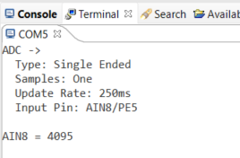
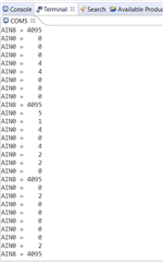
I read 8 adc0 channels using interrupt, but further i Require 9 channels , I tried with different sample sequencer, separate ISR as well as Polling all this method doesn't give me 9th channel ADC data. This is on Port E CH_8, is there any issue in configuration or something missing .
My code is based on Tiva series SDk version :- TivaWare_C_Series-2.2.0.295
and compiler is: - TI v 18.12.2.LTS
Please Help.
Regards
Khodidas
#include <stdint.h>
#include <stdbool.h>
#include <stdio.h>
//#include "inc/tm4c1294ncpdt.h"
#include "driverlib/comp.h"
#include "inc/hw_ints.h"
#include "inc/hw_memmap.h"
#include "inc/hw_adc.h"
#include "inc/hw_types.h"
#include "inc/hw_udma.h"
#include "inc/hw_emac.h"
#include "driverlib/debug.h"
#include "driverlib/gpio.h"
#include "driverlib/interrupt.h"
#include "driverlib/pin_map.h"
#include "driverlib/sysctl.h"
#include "driverlib/uart.h"
#include "driverlib/adc.h"
#include "driverlib/udma.h"
#include "driverlib/emac.h"
#include "driverlib/flash.h"
//#define TARGET_IS_BLIZZARD_RB1
#include "driverlib/rom.h"
#include "driverlib/ssi.h"
void gpioread();
//================================SPI SLAVE INITIALIZATION====================//
#define NUM_SSI_DATA 5
uint32_t pui32DataTx[NUM_SSI_DATA];
uint32_t pui32DataRx[NUM_SSI_DATA];
uint32_t ui32Index;
uint32_t adcBuffer2[9];
uint32_t ui32SysClock=0;
bool in[25];
//
// Interrupt Handler ADC0SS0
//
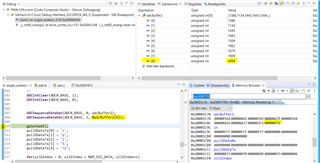
void ADC0IntHandler(void)
{
// Clear interrupt Flag
ADCIntClear(ADC0_BASE, 0);
ADCSequenceDataGet(ADC0_BASE, 0, adcBuffer2);
}
void adc2_init(void)
{
uint32_t adcClock=0, adcDiv=0;
// Enable the ADC0 peripheral
SysCtlPeripheralEnable(SYSCTL_PERIPH_ADC0);
SysCtlPeripheralEnable(SYSCTL_PERIPH_GPIOD);
GPIOPinTypeADC(GPIO_PORTD_BASE, GPIO_PIN_7 | GPIO_PIN_6 | GPIO_PIN_5 | GPIO_PIN_4 | GPIO_PIN_3| GPIO_PIN_2| GPIO_PIN_1 | GPIO_PIN_0);
SysCtlPeripheralEnable(SYSCTL_PERIPH_GPIOE);
GPIOPinTypeADC(GPIO_PORTE_BASE, GPIO_PIN_5);// | GPIO_PIN_1 | GPIO_PIN_2 | GPIO_PIN_3);
// Configure the ADC to use PLL at 480 MHz with Full rate devided by 30 to get 16 MHz
ADCClockConfigSet(ADC0_BASE, ADC_CLOCK_SRC_PLL | ADC_CLOCK_RATE_FULL, 15);
ADCSequenceDisable(ADC0_BASE, 0);
ADCSequenceDisable(ADC0_BASE, 1);
// Read the current ADC configuration
adcClock=ADCClockConfigGet(ADC0_BASE, &adcDiv);
// Hardware averageing: by a faktor of 2 -> 2,4,8,16,32,64
ADCHardwareOversampleConfigure(ADC0_BASE, 8);
// ADC voltage-lvl reference set to intern
ADCReferenceSet(ADC0_BASE, ADC_REF_INT);
ADCReferenceSet(ADC0_BASE, ADC_REF_INT);
// ADC Sequencer config: Source ADC0, Sequencer 0, Trigger: always, priority: 0
ADCSequenceConfigure(ADC0_BASE, 0, ADC_TRIGGER_ALWAYS, 0);
ADCSequenceConfigure(ADC0_BASE, 1, ADC_TRIGGER_ALWAYS, 1);
// ADC Sequencer step
// 1. Source-ADC -> ADC0_BASE
// 2. Source-Sequencer -> 0
// 3. Sample-Value depends in the depth of the FIFO, by Sequencer 0 it is up to 7 (0-7)
// 4. Config-> select input-channel AINx, interrupt specification
//
ADCSequenceStepConfigure(ADC0_BASE, 1, 0, ADC_CTL_CH8 |ADC_CTL_IE|ADC_CTL_END);
ADCSequenceStepConfigure(ADC0_BASE, 0, 0, ADC_CTL_CH4);
ADCSequenceStepConfigure(ADC0_BASE, 0, 1, ADC_CTL_CH5);
ADCSequenceStepConfigure(ADC0_BASE, 0, 2, ADC_CTL_CH6);
ADCSequenceStepConfigure(ADC0_BASE, 0, 3, ADC_CTL_CH7);
ADCSequenceStepConfigure(ADC0_BASE, 0, 4, ADC_CTL_CH12);
ADCSequenceStepConfigure(ADC0_BASE, 0, 5, ADC_CTL_CH13);
ADCSequenceStepConfigure(ADC0_BASE, 0, 6, ADC_CTL_CH14);
ADCSequenceStepConfigure(ADC0_BASE, 0, 7, ADC_CTL_CH15 |ADC_CTL_IE|ADC_CTL_END );
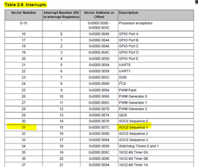
IntPrioritySet(INT_ADC0SS0, 0x00);
// ADC0SS0 Interrupt source
ADCIntRegister(ADC0_BASE, 0, ADC0IntHandler);
// Register Interrupt to NVIC
IntRegister(INT_ADC0SS0, ADC0IntHandler);
// ADC0 enable
ADCIntEnable(ADC0_BASE, 0);
// Interrupt ADC0SS0 enable
IntEnable(INT_ADC0SS0);
// Enable Global Interrupts
IntMasterEnable();
ADCSequenceEnable(ADC0_BASE, 0);
ADCSequenceEnable(ADC0_BASE, 1);
}
void SPI_Init()
{
// The SSI0 peripheral must be enabled for use.
SysCtlPeripheralEnable(SYSCTL_PERIPH_SSI0);
SysCtlPeripheralEnable(SYSCTL_PERIPH_GPIOA);
GPIOPinConfigure(GPIO_PA2_SSI0CLK);
GPIOPinConfigure(GPIO_PA3_SSI0FSS);
GPIOPinConfigure(GPIO_PA4_SSI0XDAT0);
GPIOPinConfigure(GPIO_PA5_SSI0XDAT1);
GPIOPinTypeSSI(GPIO_PORTA_BASE, GPIO_PIN_5 | GPIO_PIN_4 | GPIO_PIN_3 | GPIO_PIN_2);
// Configure and enable the SSI port for SPI master mode. Use SSI0, system clock supply, idle clock level low and active low clock in
// freescale SPI mode, master mode, 1MHz SSI frequency, and 8-bit data.
// For SPI mode, you can set the polarity of the SSI clock when the SSI unit is idle. You can also configure what clock edge you want to
// capture data on. Please reference the datasheet for more information on the different SPI modes.
SSIConfigSetExpClk(SSI0_BASE, ui32SysClock, SSI_FRF_MOTO_MODE_0, SSI_MODE_SLAVE, 1000000, 8);
// Enable the SSI0 module.
SSIEnable(SSI0_BASE);
}
void digital_init()
{
SysCtlPeripheralEnable(SYSCTL_PERIPH_GPION); // FOR LED
GPIOPinTypeGPIOOutput(GPIO_PORTN_BASE, GPIO_PIN_1);
GPIODirModeSet(GPIO_PORTN_BASE,GPIO_PIN_1,GPIO_DIR_MODE_OUT);
GPIOPinWrite(GPIO_PORTN_BASE, GPIO_PIN_1, 0x02);
GPIOPinWrite(GPIO_PORTN_BASE, GPIO_PIN_1, 0x02);
//===========================Output Pins==============================//
SysCtlPeripheralEnable(SYSCTL_PERIPH_GPIOA);
GPIOPinTypeGPIOOutput(GPIO_PORTA_BASE, GPIO_PIN_0 |GPIO_PIN_1 );
GPIODirModeSet(GPIO_PORTA_BASE,GPIO_PIN_0 |GPIO_PIN_1 ,GPIO_DIR_MODE_OUT);
SysCtlPeripheralEnable(SYSCTL_PERIPH_GPIOC);
//GPIOUnlockPin(GPIO_PORTC_BASE, GPIO_PIN_4);
GPIOPinTypeGPIOOutput(GPIO_PORTC_BASE, GPIO_PIN_4 |GPIO_PIN_5 |GPIO_PIN_6|GPIO_PIN_7 );
GPIODirModeSet(GPIO_PORTC_BASE,GPIO_PIN_4 |GPIO_PIN_5 |GPIO_PIN_6|GPIO_PIN_7,GPIO_DIR_MODE_OUT);
SysCtlPeripheralEnable(SYSCTL_PERIPH_GPIOK);
GPIOPinTypeGPIOOutput(GPIO_PORTK_BASE, GPIO_PIN_0 |GPIO_PIN_1 |GPIO_PIN_2 |GPIO_PIN_3 |GPIO_PIN_4 |GPIO_PIN_5 |GPIO_PIN_6|GPIO_PIN_7 );
GPIODirModeSet(GPIO_PORTK_BASE,GPIO_PIN_0 |GPIO_PIN_1 |GPIO_PIN_2 |GPIO_PIN_3 |GPIO_PIN_4 |GPIO_PIN_5 |GPIO_PIN_6|GPIO_PIN_7 ,GPIO_DIR_MODE_OUT);
SysCtlPeripheralEnable(SYSCTL_PERIPH_GPIOP);
GPIOPinTypeGPIOOutput(GPIO_PORTP_BASE, GPIO_PIN_0 |GPIO_PIN_1 |GPIO_PIN_2 |GPIO_PIN_3 |GPIO_PIN_4 |GPIO_PIN_5 );
GPIODirModeSet(GPIO_PORTP_BASE,GPIO_PIN_0 |GPIO_PIN_1 |GPIO_PIN_2 |GPIO_PIN_3 |GPIO_PIN_4 |GPIO_PIN_5 ,GPIO_DIR_MODE_OUT);
SysCtlPeripheralEnable(SYSCTL_PERIPH_GPIOQ);
GPIOPinTypeGPIOOutput(GPIO_PORTQ_BASE, GPIO_PIN_0 |GPIO_PIN_1 |GPIO_PIN_2 |GPIO_PIN_3 |GPIO_PIN_4 );
GPIODirModeSet(GPIO_PORTQ_BASE,GPIO_PIN_0 |GPIO_PIN_1 |GPIO_PIN_2 |GPIO_PIN_3 |GPIO_PIN_4 ,GPIO_DIR_MODE_OUT);
//===========================Input Pins PORT L,M, F, G ,J==============================//
SysCtlPeripheralEnable(SYSCTL_PERIPH_GPIOL);
GPIOPinTypeGPIOInput(GPIO_PORTL_BASE, GPIO_PIN_0 |GPIO_PIN_1|GPIO_PIN_2|GPIO_PIN_3|GPIO_PIN_4|GPIO_PIN_5|GPIO_PIN_6|GPIO_PIN_7 );
GPIODirModeSet(GPIO_PORTL_BASE,GPIO_PIN_0 |GPIO_PIN_1|GPIO_PIN_2|GPIO_PIN_3|GPIO_PIN_4|GPIO_PIN_5|GPIO_PIN_6|GPIO_PIN_7,GPIO_DIR_MODE_IN);
SysCtlPeripheralEnable(SYSCTL_PERIPH_GPIOM);
GPIOPinTypeGPIOInput(GPIO_PORTM_BASE, GPIO_PIN_0 |GPIO_PIN_1|GPIO_PIN_2|GPIO_PIN_3|GPIO_PIN_4|GPIO_PIN_5|GPIO_PIN_6|GPIO_PIN_7 );
GPIODirModeSet(GPIO_PORTM_BASE,GPIO_PIN_0 |GPIO_PIN_1|GPIO_PIN_2|GPIO_PIN_3|GPIO_PIN_4|GPIO_PIN_5|GPIO_PIN_6|GPIO_PIN_7,GPIO_DIR_MODE_IN);
SysCtlPeripheralEnable(SYSCTL_PERIPH_GPIOF);
GPIOPinTypeGPIOInput(GPIO_PORTF_BASE, GPIO_PIN_0 |GPIO_PIN_1|GPIO_PIN_2|GPIO_PIN_3|GPIO_PIN_4);
GPIODirModeSet(GPIO_PORTF_BASE,GPIO_PIN_0 |GPIO_PIN_1|GPIO_PIN_2|GPIO_PIN_3|GPIO_PIN_4,GPIO_DIR_MODE_IN);
SysCtlPeripheralEnable(SYSCTL_PERIPH_GPIOG);
GPIOPinTypeGPIOInput(GPIO_PORTG_BASE, GPIO_PIN_0 |GPIO_PIN_1);
GPIODirModeSet(GPIO_PORTG_BASE,GPIO_PIN_0 |GPIO_PIN_1,GPIO_DIR_MODE_IN);
SysCtlPeripheralEnable(SYSCTL_PERIPH_GPIOJ);
GPIOPinTypeGPIOInput(GPIO_PORTJ_BASE, GPIO_PIN_0 |GPIO_PIN_1);
GPIODirModeSet(GPIO_PORTJ_BASE,GPIO_PIN_0 |GPIO_PIN_1,GPIO_DIR_MODE_IN);
}
void main(void)
{
ui32SysClock=SysCtlClockFreqSet(SYSCTL_OSC_INT | SYSCTL_USE_PLL | SYSCTL_CFG_VCO_480, 120000000);
// ADC Init
adc2_init();
digital_init();
SPI_Init();
while(1)
{
GPIOPinWrite(GPIO_PORTN_BASE, GPIO_PIN_1, 0x02);
GPIOPinWrite(GPIO_PORTA_BASE, GPIO_PIN_0, 0x01);
GPIOPinWrite(GPIO_PORTA_BASE, GPIO_PIN_1, 0x02);
GPIOPinWrite(GPIO_PORTC_BASE, GPIO_PIN_4, 0x10);
GPIOPinWrite(GPIO_PORTC_BASE, GPIO_PIN_5, 0x20);
GPIOPinWrite(GPIO_PORTC_BASE, GPIO_PIN_6, 0x40);
GPIOPinWrite(GPIO_PORTC_BASE, GPIO_PIN_7, 0x80);
GPIOPinWrite(GPIO_PORTK_BASE, GPIO_PIN_0, 0x01);
GPIOPinWrite(GPIO_PORTK_BASE, GPIO_PIN_1, 0x02);
GPIOPinWrite(GPIO_PORTK_BASE, GPIO_PIN_2, 0x04);
GPIOPinWrite(GPIO_PORTK_BASE, GPIO_PIN_3, 0x08);
GPIOPinWrite(GPIO_PORTK_BASE, GPIO_PIN_4, 0x10);
GPIOPinWrite(GPIO_PORTK_BASE, GPIO_PIN_5, 0x20);
GPIOPinWrite(GPIO_PORTK_BASE, GPIO_PIN_6, 0x40);
GPIOPinWrite(GPIO_PORTK_BASE, GPIO_PIN_7, 0x80);
GPIOPinWrite(GPIO_PORTP_BASE, GPIO_PIN_0, 0x01);
GPIOPinWrite(GPIO_PORTP_BASE, GPIO_PIN_1, 0x02);
GPIOPinWrite(GPIO_PORTP_BASE, GPIO_PIN_2, 0x04);
GPIOPinWrite(GPIO_PORTP_BASE, GPIO_PIN_3, 0x08);
GPIOPinWrite(GPIO_PORTP_BASE, GPIO_PIN_4, 0x10);
GPIOPinWrite(GPIO_PORTP_BASE, GPIO_PIN_5, 0x20);
GPIOPinWrite(GPIO_PORTQ_BASE, GPIO_PIN_0, 0x01);
GPIOPinWrite(GPIO_PORTQ_BASE, GPIO_PIN_1, 0x02);
GPIOPinWrite(GPIO_PORTQ_BASE, GPIO_PIN_2, 0x04);
GPIOPinWrite(GPIO_PORTQ_BASE, GPIO_PIN_3, 0x08);
GPIOPinWrite(GPIO_PORTQ_BASE, GPIO_PIN_4, 0x10);
SysCtlDelay(ui32SysClock/12);
GPIOPinWrite(GPIO_PORTN_BASE, GPIO_PIN_1, 0x00);
GPIOPinWrite(GPIO_PORTA_BASE, GPIO_PIN_0, 0x00);
GPIOPinWrite(GPIO_PORTA_BASE, GPIO_PIN_1, 0x00);
GPIOPinWrite(GPIO_PORTC_BASE, GPIO_PIN_4, 0x00);
GPIOPinWrite(GPIO_PORTC_BASE, GPIO_PIN_5, 0x00);
GPIOPinWrite(GPIO_PORTC_BASE, GPIO_PIN_6, 0x00);
GPIOPinWrite(GPIO_PORTC_BASE, GPIO_PIN_7, 0x00);
GPIOPinWrite(GPIO_PORTK_BASE, GPIO_PIN_0, 0x00);
GPIOPinWrite(GPIO_PORTK_BASE, GPIO_PIN_1, 0x00);
GPIOPinWrite(GPIO_PORTK_BASE, GPIO_PIN_2, 0x00);
GPIOPinWrite(GPIO_PORTK_BASE, GPIO_PIN_3, 0x00);
GPIOPinWrite(GPIO_PORTK_BASE, GPIO_PIN_4, 0x00);
GPIOPinWrite(GPIO_PORTK_BASE, GPIO_PIN_5, 0x00);
GPIOPinWrite(GPIO_PORTK_BASE, GPIO_PIN_6, 0x00);
GPIOPinWrite(GPIO_PORTK_BASE, GPIO_PIN_7, 0x00);
GPIOPinWrite(GPIO_PORTP_BASE, GPIO_PIN_0, 0x00);
GPIOPinWrite(GPIO_PORTP_BASE, GPIO_PIN_1, 0x00);
GPIOPinWrite(GPIO_PORTP_BASE, GPIO_PIN_2, 0x00);
GPIOPinWrite(GPIO_PORTP_BASE, GPIO_PIN_3, 0x00);
GPIOPinWrite(GPIO_PORTP_BASE, GPIO_PIN_4, 0x00);
GPIOPinWrite(GPIO_PORTP_BASE, GPIO_PIN_5, 0x00);
GPIOPinWrite(GPIO_PORTQ_BASE, GPIO_PIN_0, 0x00);
GPIOPinWrite(GPIO_PORTQ_BASE, GPIO_PIN_1, 0x00);
GPIOPinWrite(GPIO_PORTQ_BASE, GPIO_PIN_2, 0x00);
GPIOPinWrite(GPIO_PORTQ_BASE, GPIO_PIN_3, 0x00);
GPIOPinWrite(GPIO_PORTQ_BASE, GPIO_PIN_4, 0x00);
SysCtlDelay(ui32SysClock/12);
//ADCSequenceDataGet(ADC0_BASE, 0, adcBuffer2);
ADCSequenceDataGet(ADC0_BASE, 1, &adcBuffer2[9]);
gpioread();
pui32DataTx[0] = 's';
pui32DataTx[1] = 'p';
pui32DataTx[2] = 'I';
pui32DataTx[3] = 'S';
pui32DataTx[4] = '\n';
for(ui32Index = 0; ui32Index < NUM_SSI_DATA; ui32Index++)
{
// Send the data using the "blocking" put function. This function
// will wait until there is room in the send FIFO before returning.
// This allows you to assure that all the data you send makes it into
// the send FIFO.
//
SSIDataPutNonBlocking(SSI0_BASE, pui32DataTx[ui32Index]);
//SSIDataGet(SSI0_BASE, &pui32DataRx[ui32Index]);
SSIDataGetNonBlocking(SSI0_BASE, &pui32DataRx[ui32Index]);
}
}
}
void gpioread()
{
in[0]=GPIOPinRead(GPIO_PORTL_BASE, GPIO_PIN_0);
in[1]=GPIOPinRead(GPIO_PORTL_BASE, GPIO_PIN_1);
in[2]=GPIOPinRead(GPIO_PORTL_BASE, GPIO_PIN_2);
in[3]=GPIOPinRead(GPIO_PORTL_BASE, GPIO_PIN_3);
in[4]=GPIOPinRead(GPIO_PORTL_BASE, GPIO_PIN_4);
in[5]=GPIOPinRead(GPIO_PORTL_BASE, GPIO_PIN_5);
in[6]=GPIOPinRead(GPIO_PORTL_BASE, GPIO_PIN_6);
in[7]=GPIOPinRead(GPIO_PORTL_BASE, GPIO_PIN_7);
in[8]=GPIOPinRead(GPIO_PORTM_BASE, GPIO_PIN_0);
in[9]=GPIOPinRead(GPIO_PORTM_BASE, GPIO_PIN_1);
in[10]=GPIOPinRead(GPIO_PORTM_BASE, GPIO_PIN_2);
in[11]=GPIOPinRead(GPIO_PORTM_BASE, GPIO_PIN_3);
in[12]=GPIOPinRead(GPIO_PORTM_BASE, GPIO_PIN_4);
in[13]=GPIOPinRead(GPIO_PORTM_BASE, GPIO_PIN_5);
in[14]=GPIOPinRead(GPIO_PORTM_BASE, GPIO_PIN_6);
in[15]=GPIOPinRead(GPIO_PORTM_BASE, GPIO_PIN_7);
in[16]=GPIOPinRead(GPIO_PORTF_BASE, GPIO_PIN_0);
in[17]=GPIOPinRead(GPIO_PORTF_BASE, GPIO_PIN_1);
in[18]=GPIOPinRead(GPIO_PORTF_BASE, GPIO_PIN_2);
in[19]=GPIOPinRead(GPIO_PORTF_BASE, GPIO_PIN_3);
in[20]=GPIOPinRead(GPIO_PORTF_BASE, GPIO_PIN_4);
in[21]=GPIOPinRead(GPIO_PORTG_BASE, GPIO_PIN_0);
in[22]=GPIOPinRead(GPIO_PORTG_BASE, GPIO_PIN_1);
in[23]=GPIOPinRead(GPIO_PORTJ_BASE, GPIO_PIN_0);
in[24]=GPIOPinRead(GPIO_PORTJ_BASE, GPIO_PIN_1);
}