Part Number: TM4C1294NCPDT
Other Parts Discussed in Thread: UNIFLASH
This post is about a custom board with a TM4C1294NCPDT. This product has just gone into Revision B, and the JTAG connections are a copy/paste of the same schematics successfully used in many other products of the company.
A batch of 5 boards was produced, and none of them will accept the JTAG connection for firmware transfer and debugging.
The following "emulators" or probes were tried:
- IDCI from a TM4C1294 Launchpad
- XDS100v2
- XDS200
All of these pods properly apply firmware and debug other boards with similar configurations.
The following software was tried to connect to the boards:
- Directly from CCSv7.1
- LMFlash
- UniFlash
The error on CCS is:
"CORTEX_M4_0: Error connecting to the target: (Error -2062 @ 0x0) Unable to halt device."
Trying to apply the unlock solution from UniFlash or LMFlash did not result.
The following was tested on HW level:
- Power into the MCU is confirmed 3.3V on all of the VDD labeled pins, namely 7, 16, 26, 28, 39, 47, 51, 52, 69, 79, 90, 101, 113, 122. VDDA and VBAT are also on the same power bus at 3.3V.
- No neighbor pin is shorted or showing 3V3.
- VREFA+ is powered by 3.0V
- All GND/GNDA pins were checked for shorts and confirmed to be properly connected to ground, namely 10, 17, 48, 55, 58, 80, 114.
- The VDDC lines are measure to be ~1.2V as expected.
- #HIB is floating
- #WAKE is WPD to GND via 10K
- #RESET is WPU to 3V3 via 10K and into a board's reset button as well as to JTAG reset line. The other end of the button is connected to GND, and pushing the reset button properly brings the #RESET line to GND as expected, suggesting that there is nothing "locking the reset high".
- TMS, TCK, TDO, TDI, GND and VTARG are all double checked to their respective MCU pins and into JTAG connector.
- Board current without firmware and no other functions enabled are within reasonable, at 30mA.
- No unreasonable voltage on any of the other pins of the MCU.
Using a scope on TCK, I can see an initial nice train of pulses on TCK, with square edges and true at 1MHz. Then it stops for a while and try again, before dying. There was no time today to view the other signals.
We do not use WPU's on the JTAG lines - never used, never had a problem - but recently accepted the suggestion and will do from now on. On two of these boards, we added 4 WPU's (3K3) on TMS, TCK, TDO, TDI. To no avail.
As I write this, I'm reading the JTAG document spma075.pdf. The following aspects are learned and are different from the current status:
- JTAG pull-up resistors shall be 10K, not 3K3.
- The pull resistor on TDO is actually PULL-DOWN, not Up. Some non-official comments on the forum mislead this information.
- There shall be no pull-up on TDI
If the above fixes don't solve it, the following can still be done:
- Check at OSC0 pin that the crystal is properly oscillating.
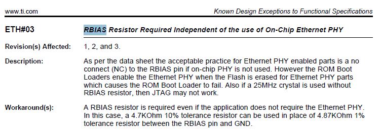
- Make sure RBIAS resistor is properly populated... We DO NOT have RBIAS resistor, for this board does not use Ethernet. Datasheet says that preferred practice for unused RBIAS pin is NC. However, yes, there IS a 25MHz crystal into OSC0... Question 1: Could that be this exact problem?
Question2: where can I find the meaning for ERROR -2062 and other JTAG error codes?
More later, hopefully tomorrow.