This thread has been locked.

If you have a related question, please click the "Ask a related question" button in the top right corner. The newly created question will be automatically linked to this question.

DRV8350R: Vds OCP false triggering during testing on Vehicle

Part Number: DRV8350R
Other Parts Discussed in Thread: DRV8350, CSD19535KCS

We are designing a 1 Kw BLDC motor drive using drv8350R for a three wheeler vehicle.

The layout and schematics were designed in two iterations and the 2nd iteration was designed based on the suggestions from the E2E forum and was also uploaded for verification.

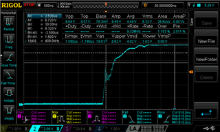
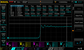
The boards were manufactured and the boards were operating perfectly. We loaded the boards upto 1.7 Kw on a dynamometer. Initially we faced issues with false triggering of Vds OCP, and we kind of solved it by increasing the drive current but to make it work the vds ocp level was set at least 6 times more than the theoretical calculated values. 

After that when we started testing the boards on the actual vehicle, the vds ocp would still get triggered even with maximum deglitch time settings and increased drive current. The same boards are working on dynamometer, but not on the actual vehicle. 

The Vds OCP is false triggering much earlier on the vehicle, even if the ocp levels are set at very high values.

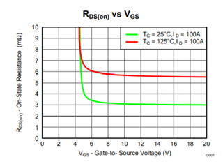
The mosfet which we are using has 13nC Qgd and 3.1 mOhm RdsOn.

Gate drive current is set at 400/800 mA. 

 I know voltage waveforms are required for this but it's difficult to take waveforms on a moving vehicle.

I have attached the layout and the schematic for the inverter circuit.

Refer this for layout: 7455.Power_Board_V2.pdf

Refer This for schematic only:VCU_MCU_V2.pdf

  • Hi Yashdeep,


    Thank you for posting your question on the Motor Drivers forum!

    Could you induce a VDS fault and then record the value of the Fault Status Register 1 register (particularly bits 0-5), and then repeat this multiple times to see if the VDS fault occurs on: 

    1. all phases (both high side and low side)

    2. Only on high side FETs

    3. Only on low side FETs

    or

    4. Only on 1 particular phase

    If the VDS fault always only occurs on one particular phase (such as phase A) then it could point to a layout issue with that particular phase (maybe a result of higher parasitic inductance). If the fault only occurs on the high side FETs or only on the low side FETs, that could also indicate a layout issue that causes the low side or high side VDS voltage to not be sensed properly. The high side VDS voltage is monitored from the Vdrain pin to the SHx pin, and the low side VDS voltage is monitored from the SHx pin to the SPx pin. So if there is high inductance (which is effected by the number of vias used, the thickness of the trace, and the length of the trace) in the trace from the pin to the half bridge connection, or if the trace is long, this can effect the accuracy of the voltage sensed at the pins that are used for VDS monitoring. 

    What is the Vin supply voltage for your design? What is the anticipated amount of current that is flowing through the FETs? Is there a way to measure the actual current flowing through a particular phase when a VDS overcurrent event occurs? What VDS voltage are you using?

    The IDRIVE setting that you are using currently (400mA/800mA) is quite high based on the Qgd of the FET you are using and could lead to ringing on the gate and source of the FETs. Most customers would consider 100ns -200ns turn on time a fast turn on time, and with the current setting the turn on time would be about 13nC/400mA = 32.5nS, though the value of the gate resistor would effect the turn on time. If you don't see much ringing on the gate and/or source of the FET while switching on or off with this IDRIVE setting, then it is probably ok. But if there is quite a bit of ringing then this will result in EMI concerns and could possibly lead to damage to the Gate or source pins if the voltage ratings of the device are exceeded. Additionally, if the voltage oscillation occurs for a period of time longer than the deglitch time, then this could contribute to inaccurate VDS monitoring.

    Regards,

    Anthony

  • Hello Anthony,

    Sorry for the delayed response.

    I induced several vds faults as you suggested, and noticed that almost every time the faults occured on the high side mosfets. These faults were some times ocp and sometimes gate drive faults.

    These are happening as soon as I am starting the vehicle when the drive current is 150 ma and if I increase the drive current to 400 ma, then it works for some duration before the faults are triggered.

    I want to emphasize again, that the same board was working completely fine on the test rig where we loaded it upto 45 amps for 30 secs.

    The layout was optimised as much as possible given the limits of two layers of pcb and mosfet package.

    The Vin supply ranges from 48 -53V and the expected peak current for a phase could go upto 80 amps for a  very short duration of time, but the continuous rating is around 30 amps. I was not able to measure the the current at the time of tripping. What do you mean by Vgs voltage?

    I probed the voltage at the Vdrain rail and observed a dip of around 4V for 200 ns at the time of switching. I have thought of putting a 0.1 uf cap between the vdrain pin and the ground. Will this work?

    I have also removed the gate resistors but noticed no improvement. 

    My bulk capacitors and bypass capacitors are connected between vdrain and gnd( after sense resistor),which is not in accordance with the reference design for drv8350, where these caps are connected before the sense resistors.

    Kindly look at this also:

    manufactured and the boards were operating perfectly. We loaded the boards upto 1.7 Kw on a dynamometer. Initially we faced issues with false triggering of Vds OCP, and we kind of solved it by increasing the drive current but to make it work the vds ocp level was set at least 6 times more than the theoretical calculated values. 
  • Hi Yashdeep,

    Anthony will get back to you early next week

    Thanks,

    Matt

  • Hi Yashdeep,

    Thank you for the additional information! what I meant by Vds voltage is the VDS overcurrent protection voltage setting that is being used. this can be found in the VDS_LVL bits of the OCP control register. This voltage determines the voltage drop across the drain to source of the MOSFET that is required to trigger the overcurrent protection. 

    Regarding the 4V droop in the power supply rail during the switching of the MOSFET: you could add a 0.1uF capacitor here, but I would recommend increasing it to at least 1uF. It is best to have this as close to the half bridge as possible. Additionally, it seems like your system might need more bulk capacitance. If this is possible, it may help keep the supply voltage more stable.

    Here are a couple of observations that I have:

    1. You mentioned that you had a similar issue of the VDS overcurrent triggering when testing it out on a dynamometer, and in order to resolve the issue you had to increase the VDS OCP level at least 6 times higher than the theoretical calculated values. This could indicate a few things:

        a. The voltage sensed at the VDRAIN pin of the driver is not accurately measuring the voltage that is at the drain of the FET, such that the Vds voltage appears to be greater than it actually is. Another possibility is that the voltage at the SHx pin is not accurately reflecting the actual voltage of the switch node and is causing the Vds voltage to appear greater than it actually is.

       b. The actual voltage across the high side FETs is higher than what would be expected, possibly due to the high side FET not being fully enhanced.

    When I look at the PCB layout, one thing that I see that potentially could be problematic is that the VDRAIN traces are routed underneath some switching traces such as the gate traces and the high side source traces. I wonder if there possibly could be some coupling that could be occurring due to the switching on the other phases that could be coupling on to the VDRAIN trace, giving it a higher than expected voltage reading. You may try soldering on a thick insulated wire to have a better connection from the drain of the high side FETs to the VDRAIN pin to see if this improves anything. 

    What environment are you testing out the 3 wheeler vehicle in? I am pretty sure the root cause is the same issue that was seen on the dynamometer. In the first testing with the dynamometer, you were able to fix it by increasing the VDS voltage threshold, however in the new testing the higher VDS voltage threshold didn't fix the issue probably because there is a lot more opportunity for more variation in torque at a faster rate especially if it is being operated on uneven surfaces. It is possible that the torque applied to the 3 wheeler in a real use case could be applied much quicker and have more variation than what was simulated on the dynamometer. This would cause faster change in current as well as a greater increase in the back emf voltage, and potentially could be causing some voltage change on the switch node that could falsely trigger the VDS protection circuitry. 

    Would it be possible to get some waveforms showing the gate to source voltage of one of the high side FETs as well as the high side source to ground voltage? I want to see if there is any issue with the FETs being able to fully turn on. Additionally, If you are able to measure the VDS voltage that would be helpful. It would be a good idea (if you are able) to switch back to do some testing on the dynamometer, and then see if we can resolve that issue with a better solution then simply increasing the VDS voltage level. This may help us resolve the issue you are seeing during operation of the 3 wheeler vehicle. 

    You mentioned that the motor could run for some time before a fault occurred as long as your drive current was high enough. How long does it take for a fault to occur? Does it correspond with a particular event (maybe during fast acceleration or uneven surfaces)?

    Regards,

    Anthony 

  • Hello Anthony,

    Sorry for the lte reply,

    I was out of office for some days. There was a misunderstanding about the vds level, it's not 6 times but only around maybe 2 or 3 times the theoretical  value, currently we have set the vds level at 1 volts. The mosfet which we are using has 3.1 mohms Rdson at 25degrees Celsius. Our design requires dc current of 50 amps, and around 120 amps phase current ( at lower duty cycle). We were able to operate the vehicle under lenient conditions by implementing current limiting for each phase at around 42 amps, but that is not enough since our requirement needs around 120 amps peak for max of 30 secs. And if we are increasing the current limiting set point to a higher value, say 50 amps and try to increase the speed (duty cycle), the vds ocp would trigger. Today, on the test rig, same issue was there so we increased the vds ocp to 1.5 V and one of the lower mosfets got damaged. The mosfet is rated for 187 amps continuous at 25degrees and 130 amps continuous at 100degrees with peak pulse rating of 400 amps.

    Mosfet No.CSD19535KCS

    We have not yet taken the waveforms like you asked for. I have asked my team to do that and I will share it here asap. 

    One more things I noticed in our design was that the VM pin is being supplied at 10.3 volts whereas the reference design in data sheet has 12 volts supply for vm. Could this be an issue?

  • Hi Yashdeep,

    Thank you for the additional information! It is fine to operate the driver with a VM of 10.3V, but one thing to keep in mind is that this will result in a lower VCP and VGLS voltage as shown in the datasheet, which means that the high side gate to source voltage will only be enhanced to about 8V instead of 10V.

    This will increase the Rds(on) resistance a little bit, but not substantially (maybe by a few hundred micro ohms). Notice that as the MOSFET temperature increases there is a substantial rise in Rds(on), but this is still not sufficient to explain why the VDS monitoring is tripping with such a high setting.

    You mention that you set current limiting to around 42A and then later adjusted it to 50A. Could you walk me through how you calculated the threshold for current limiting? If you implementing current limiting through the DRV, this is done as follows:

    1. the OCP_MODE bits of the OCP control register must be 01b (which is default the setting)

    2. the CBC bit of the Gate Drive LS register must be 1b (which is default the setting) 

    3. the OCP_ACT bit of the Driver Control register must be 0b (which is default the setting) 

    4. Determine the peak current desired for current limiting (taking into account the deglitch time)

    5. Chose a sense resistor value and set the SEN_LVL bits of the CSA Control register to set the voltage trip threshold such that:

               Sense Level Voltage = trip current x sense resistor resistance.

    SEN_LVL has 4 available settings: 0.25V, 0.5V, 0.75V, and 1V. If you are using the same sense resistor as in the schematic (3.5m ohms), then if you set a trip voltage of 42A you would need a sense level voltage of 42A*3.5m ohms = 0.147V, which is not a value that is available for this device (0.25V is the lowest setting). In order to perform current limiting at 42A, it would be necessary to change the sense resistor to about 6m ohms. When operating the device in current limiting mode, cycle by cycle current limiting occurs when either the VDS_OCP is tripped or the SEN_OCP is tripped.

    Are you using the outputs of the sense amplifiers to have a software implemented current limiting function?

    I am looking forward to seeing the results of the waveforms,

    Anthony 

  • Thank you for the reply!

    Till now I was using VDS ocp and sense OCP just for cut-off and not limiting as I didn't properly understand the Cycle By Cycle Limiting feature of the DRV, thanks for pointing that out, will give it a try.

    Our target for phase current limit is 100 -120 Amps, this was decided based on the readings we got while testing a commercial controller with the vehicle. For now, the current limiting was implemented in the code by reading the sense amplifier outputs and 42Amps was an arbitrary threshold value, just to check the code.

    I am now a bit concerned whether the MOSFET being used is suitable or not for our design requirements. 

    Anyways, I will share the waveforms asap.

    Regards,

    Yashdeep 

  • Hi Yashdeep,

    Glad I was able to help out in explaining the current limiting feature!

    It does seem like the current ratings of the MOSFETs you are using is fairly close to the expected peak current, especially as the MOSFETs heat up and the max continuous current ratings of the MOSFET begin to decrease. It is up to you if you want to chose a MOSFET that would give you more margin for the current rating.

    Thanks for the clarification regarding the overcurrent limiting method you are using!

    Regards,

    Anthony 

  • Hello Yashdeep,

    Is there any further help that you need on this thread? Or may I close it?

    Thanks,

    Matt

  • GHA-SHA Fall

    GHA- SHA Fall

    GHA SHA Rise

    GHA -SHA Rise

    SHA Fall

    SHA Rise

    The drive current for these waveforms was 350 mA and a gate resistor of 11 ohms. I have reduced the drive current back to 150 mA.

    Kindly comment on the ringing in the waveforms whether this is within allowable limits or not.

    Now the controller is able to handle higher loading when the current limiting is applied in the gate driver.

    Thanks for the help.

  • Hello Matt,

    I have posted a final query and the waveforms which Anthony had asked for, once I get a response I will close the thread by selecting the "This resolved my issue" option.

    Thank You.

  • Hi Yashdeep,

    Thanks for the waveforms! 

    There is definitely significant oscillation on the gate and source waveforms, suggesting the IDRIVE is too high. Additionally, the turn on time looks to be a little less than 100ns, which is quite fast. I would probably aim for a turn on time of between 150ns and 200ns. This can be done by reducing the IDRIVE and then tuning the gate resistor appropriately. If you need to use a gate resistor, I would recommend using a small value, maybe 10 ohms or less. You mentioned that you reduced the gate drive current back to 150mA. If I was understanding it correctly, you used to get a fault operating with that low of an IDRIVE, is that correct? I think you mentioned that it had to be 400mA/800mA gate current in order for there not to be a fault during startup. Was this issue resolved when you used the current limiting feature? If the driver operates well at the lower IDRIVE current then I would recommend using that, especially since the FETs are low Qgd. 

    The abs max 200ns transient SHx pin voltage is -10V (negative transient) and Vdrain + 10 (Positive transient), so it looks like the abs max voltages are not being violated, however I would still recommend reducing IDRIVE since you are seeing significant overshoot/undershoot which can cause EMI issues. 

    I am glad that the current limiting feature allows for higher loading! I would still like to figure out what is causing the VDS monitors to not read accurately, but likely that would require going back to the dynamometer and running tests and getting VDS waveforms and measuring the actual current. It is up to you if you want to go down that route.

    Regards,

    Anthony 

  • Hello, 

    I have set the drive current within limits as you recommended. While our controller is able to drive the vehicle on level road but not on gradient (starting from gradient). We tested the vehicle with a commercial controller and the phase current goes upto more than 100 amps. When we increase the current limiting threshold( Vds level=0.9), to allow the vehicle to climb the gradient, the mosfets are getting damaged. We were measuring the current using a clamp meter and the current never went above 60 amps (rms).

    The mosfets we use are CSD19535KCS, our phase current target is 100 amps( rms) 15secs. 

    Can you suggest where the problem might, drv or mosfet rating ?

  • Hi Yashdeep, 

    Is only the MOSFET getting damaged, or the driver as well? Have you tried replacing the MOSFET to see if the driver works fine? What appears damaged on the MOSFET? the drain to source? You could compare the resistance of a good device to the resistance of the bad device, measuring all the pins with respect to ground as well as with respect to each other (measuring the gate to source resistance, gate to drain resistance, and drain to source resistance). Were you able to use a clamp meter during an event that caused the MOSFETs to get damaged? If the MOSFETs didn't get damaged during the test where you were using the clamp meter then maybe the peak current is able to get higher than what you replicated when testing with a clamp meter.

    Considering the ratings of the MOSFETs, and looking at the gate voltage waveforms, It doesn't look like any voltage ratings are being exceeded. If we can rule out an overcurrent event on the MOSFETs, then the only other thing that I could think of that would cause this would be an overtemperature event.

    Regards,

    Anthony 

  • Hello,

    The Mosfets were getting damaged, all the three terminals were shorted when we removed the mosfet and probed for continuity. The gate driver is fine. The heat sink we were using was not apt for our ratings so we have replaced the heat sink with one which has better heat dissipation. We are testing it now.

    We are performing PWM on High side mosfets and the lower mosfets have no pwm, rather they are kept on for the whole commutation cycle. I wanted to know, in cbc mode whether the ocp fault clears when a new pwm pulse is recieved on any mosfet or the mosfet on which the fault was detected.

  • Hi Yashdeep,

    Thank you for the update! Hopefully the improved heat sink will help solve that issue. 

    I will have to check on whether or not the CBC fault is reset on any input PWM pulse, or just the PWM pulse of the effected phase. I will try to get back to you on that by the end of the week. One thing to note is that a CBC current fault only effects the phase that experienced the event, and does not effect the other phases operation as long as the OCP_ACT bit of the Driver Control Register is 0b (which is the default setting).

    Regards,

    Anthony Lodi

  • Hi Yashdeep, 

    I have reached out to a coworker on the team to get more clarity on how the CBC fault is reset, and am waiting for a response. If I don't have an answer by Monday then I will try to run a test in lab to figure it out. Sorry for the delay.

    Regards,

    Anthony Lodi

  • Hi Yashdeep,

    For the DRV835x devices, in CBC mode the CBC fault is cleared when an input PWM pulse is detected on any of the inputs, not just the input of the phase that resulted in the CBC overcurrent fault. 

    Regards,

    Anthony Lodi

  • Hello Anthony,

    We are updating our design by using two parallel MOSFETs. Can you please comment on the layout attached below and suggest any required changes? I have also attached 3D Model of the board for better understanding.

    I have not included any capacitor between the GHX- SHX and GLX-SPX tracks, should I include any? If yes, how should I estimate the required capacitor value.

    Few things I have kept in mind while designing the layout such as, ensuring short paths for the high current loop HS Drain and LS source, Even though the GHX, SHX, GLX, SPX, SNX  tracks are a bit longer, I have substantially increased the track width to reduce any parasitic inductance introduced due to the length. I have also ensured tight coupling between gate drive tack pairs ( GHX-SHX and GLX -SPX- SNX) by routing them very close to each other. 

    How should I select the ratings of the TVS diode which is supposed to placed at the supply side? Also, is snubber circuit required or the DRV takes care of it using the Istrong current?

    Regards, 

    Yashdeep

    Power_Board_V3.pdfPower12.pdf

  • Hi Yashdeep,

    I don't see any particular need for GHx-SHx or GLx -SPx capacitors, but if you wanted to include a footprint for it to give the additional flexibility during testing you are welcome to do so.

    Would you be able to provide the layout with each individual layer showing so that I can see the individual layer traces better?

    ISTRONG current is used to pull the gate down of a particular MOSFET to prevent that low side MOSFET or high side MOSFET from accidentally switching on during the switching of the other MOSFET due to dv/dt coupling. The switching of the high side MOSFET, for example, could cause coupling onto the low side gate and begin to turn it on. ISTRONG current is used to mitigate this effect. 

    RC snubbers are used to help mitigate ringing on the high side source node, as well as ringing across the MOSFETs. See section 4.2 of this application note for more information.

    For the TVS diode, what particular diode are you referring to? The buck diode? If you are talking about placing a diode between the high side gate to source, there is already an internal diode in the DRV.

    Regards,

    Anthony Lodi 

  • Hello Yashdeep,

    Do you have any further questions on this thread?

    Thanks,

    Matt