This thread has been locked.

If you have a related question, please click the "Ask a related question" button in the top right corner. The newly created question will be automatically linked to this question.

DRV8350R: Missing Commutation At Higher RPMs

Part Number: DRV8350R

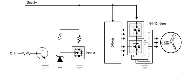
We are developing a motor controller unit using a DRV835RS5 Gate driver and DSPIC33ch Microcontroller.

The PWM frequency is set at 10KHZ and controller clock is set at 8 MHz.

The 8 pole BLDC motor has a rated RPM of 3200 at no Load 48 V.

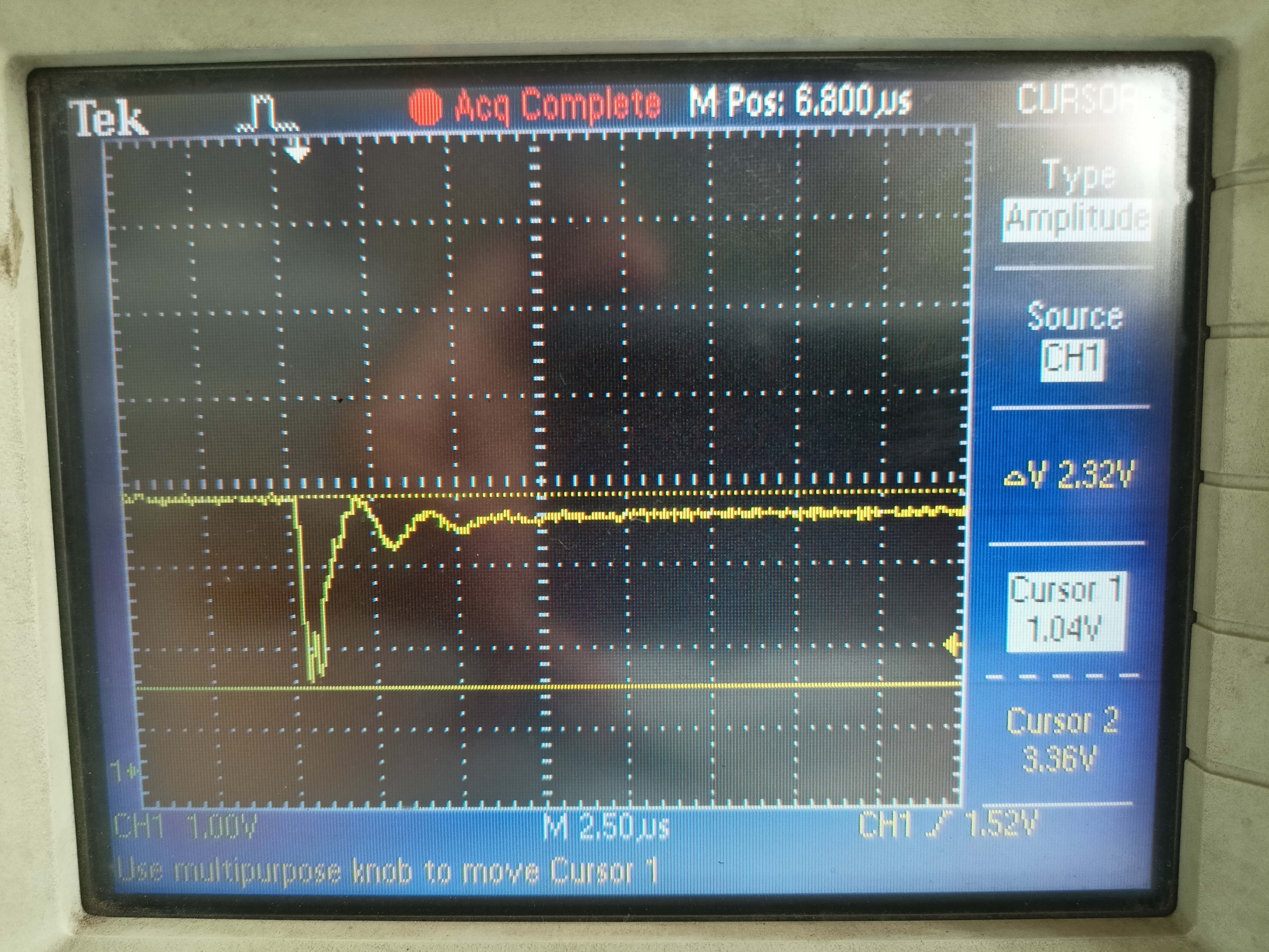
I am implementing the commutation using a Timer Interrupt which is called every 5uS.

At higher RPM (>80% DC)  the motor starts missing commutation and the gate driver stops the motoring.

The same application if implemented using polling, is working upto 85 % Duty Cycle., but I need to add extra functions  in the MCU so I have to proceed with interrupts.

Can you help rectify the problem.

  • I am also facing another issue where there is a voltage dip happening at the 3.3 V supply for the microcontroller at the exact same point in time when the mosfets are switching. As I am loading the motor and current is increasing and the dip in 3.3 rail is also increasing. It is dipping to 1.05 volts. I have even tried different power supplies but the dip is still there. This dip is causing the Microcontroller to turn off and restart. Is it due to interference from the MOSFETS switching?   BLDC_V2.4_19.07.2020.pdf

  • Hello Yashdeep,

    At higher RPM (>80% DC)  the motor starts missing commutation and the gate driver stops the motoring.

    There's a few things we can check. First, we need to see if the DRV is the problem. You need to probe INHx and INLx with a corresponding GHx and GLx to see if inputs are being received but being ignored by the DRVx. Remember, the DRVx isn't smart (in most cases), it simply looks at inputs at INx and translates them Gx. It does what it is told and if the MCU isn't telling INx to switch, then that's on the fault of the MCU (and more likely, the commutation algorithm).

    3.3 V supply for the microcontroller [is dipping] at the exact same point in time when the mosfets are switching

    This looks like it could be your problem. I didn't look up the undervoltage lockout (UVLO) spec on the MCU, but it wouldn't surprise me if this spike is causing the MCU to reset.

    There's a lot of possibilities that this could be, the most likely, based on your description, is bad layout. This is because, increased current means increased spikes on the rails. The ringing and spiking leads me to believe that the (GND) reference for the supply (or the source of the supply, which would be the buck) is bouncing around with every PWM cycle. Probing the Phase voltage to GND and lining it up with this waveform (using 2 probes, and 2 different channels on the oscilloscope) would prove this.

    Its really hard to make a judgment on your layout, but I can already tell your J16, J17, and J18 (which aren't present in the schematic you gave, by the way), are adding inductance for the traces. Remember GHx and GLx can source and sink an amp, or more of current, depending on IDRIVE settings.The SNx also act as a GND return path between the GND pin and the return path of the FETs. Actively adding inductance between these nodes means they aren't at the same potential in the case of high current traveling through (V = L*id/dt, where more L means more V)

    It also looks like you didn't pour GND on the top layer (could be wrong here), you've depopulated the parallel FETs (which leave stubs and parasitic inductance that induces more ringing), and your have placed your HS and LS FETs, what seems to be literal centimeters apparent from each other (which adds more inductance in the path). This leads me to believe you haven't read our layout guide to motor drives. I've provided it for you: https://www.ti.com/lit/an/slva959a/slva959a.pdf

    Here's an example of a reference design with 25A(RMS) at 63V that can fit the power stage into 70x69mm^2. I know most people will teach that physical isolation for a motor drive solution is preferred, but good layout is way better for decoupling noise around a circuit: https://www.ti.com/tool/TIDA-010056

    I completely understand if you don't want to try a new design. My advice is to try and continue to attach shorter, thicker, and more direct paths for current carrying paths and increase decoupling, RC snubbers, or other ringing mitigation tactics to clear up noisy GND. With whatever data you get, remember, a layout designed will be an order of magnitude better than having wires fly off the board, so take this data with the assumption that "if it gets worse, it still might be better if we do a redesign".

    Best,

    -Cole

  • Hello Cole,

    Thanks for the reply. 

    We have started working on the new layout design as per the suggestions given by you. Simultaneously we are also trying to work out the existing board to identify any new design problems which could be improved upon in the next design.

    For, now we tried connecting thick wires on the GND track of the power board as shown below. We saw a slight improvement in terms of the voltage dip due to ground bounce, but it's still there.

    So we decided to remove the gnd pin(snx) connection between the power board and the logic board(gate driver and mcu) since the snx at gate driver is already connected to the common ground of the whole system, and the dip in the 3.3 rail disappeared completely and was working fine, but as soon  as we increased the voltage, the gate drivers' charge pump for the lower side mosfets got damaged.

    Can you explain what could be the reason ?

    I believe it has something to do with ground bounce in the power board which is still there. Can you suggest any way around this so that we could complete the testing of this version of the layout? 

    Based on the problems we face, we will be designing the new layout.

  • Hello Yashdeep,

    Let me get back to you on Monday.

    Best,

    -Cole

  • Hello Yashdeep,

    The layout is still suboptimal and you haven't provided waveforms, but I'm going to assume everything is still bouncing pretty badly on the low side gate and source voltages, despite your change. Even with the spiking, we expect the DRVx to protect by triggering a fault before irreversible damage. Because the low side protection depends on SNx as a kelvin connection from the low side source to SNx pin, which you've taken that connection away, the DRV can't properly sense the change in voltage at the low side FET source. This nullifies the protection.

    You should try and see if you can lower IDRIVE to also make the voltage spiking less severe, and more likely for the DRV to survive. Use 200ns for the rise and fall time and plug it into the equation found here: Selecting the Best IDRIVE setting and Why this is Essential

    Best,

    -Cole

  • Hi, 

    I was hoping if you could suggest any cost effective reverse polarity protection scheme which also allows for regeneration current to flow back to the battery. The Smart Diode ICs like LM74610 and Lm74700 don't allow regeneration current to flow back to tbe battery.

  • Hello Yashdeep,

    Understanding the quesiton

    I just want to understand the request before I give any recommendations.

    Is the goal to have current flow back to the battery at any moment, either through the algorithm or passive components? Or is the goal to just allow current to flow back during a known condition such as braking, decelerating, or stopping?

    In addition, is the goal to recharge the battery with this current or to protect the battery by implementing something that manages the current as it flows back?

    For the case of Back EMF causing current to flow into the battery.

    I say this because the most common way for current to flow back to the battery is a result of Back EMF to be higher than the applied voltage. This usually happens in stop, coast, or decelerating commands. Usually, users are happy with  handling the current flowing back to the supply by rerouting it elsewhere.

    There are two main solution categories, algorithm based and external circuit:

    • Algorithm based solutions:
      • Measure the supply voltage during operation, and have the algorithm apply “brake” (all low-sides or high-sides ON)to the motor whenever the voltage increases above a set threshold. This will prevent the supply from pumping further
      • Limit the maximum possible deceleration in your algorithm to not apply a drive signal significantly less than the back-EMF.
      • Adjust the deceleration to include both “brake” and “coast” rather than just “coast” to mitigate some of the back-EMF
    • External circuit solutions:
      • Adding more bulk capacitance at the motor will cause the voltage to rise slower during supply pumping. Therefore, the maximum voltage that the supply rises to will decrease with additional bulk capacitance.
      • Add an external pulldown (brake circuit). This circuit can be employed to “short” the motor externally and dissipate the motor power. This is your “bleed resistor + mosfet” solution

    Best,

    -Cole

  • I am sorry, I should have framed my question in a better way. I am not worried about the reverse current to the battery, we are controlling that at the inverter itself. By Reverse Polarity protection, I meant when the user connects the board to the battery in reverse polarity accidentally, which could damage the board. Using a diode or ICs like LM74610 for this protection would then prevent the inverter from recharging the battery while braking(regen braking).

  • Also, can you comment on the new layout I have attached here, the distance between the upper and lower Msofets is 3CM.

  • Hello Yashdeep,

    Have you reviewed this app note? Let me know if it helps, if you still need more info, I'll get the smart diode team involved.

    https://www.ti.com/lit/an/slva835a/slva835a.pdf

    Best,

    -Cole

  • Hello Yashdeep,

    I believe you can upload the picture directly in the reply. We don't have access to google docs. Sorry for the inconvenience.

    Best,

    -Cole

  • Hello Yashdeep,

    Here's your layout review. By the way, please provide a matching schematic for all future layout reviews you do with anyone in the industry. It makes it easier to know what to expect.

    Layout Notes.pdf

    Best,

    -Cole

  • Hello Cole,

    Thanks a lot for giving such a detailed feedback. I have made the changes suggested by you. In some cases we were not able to follow the ideal rules due to the constraints of only 2 layers, MOSFET Package and also the pin order on the DRV. As suggested, we have increased the width of the drive signal traces to 20mil to reduce parasitic inductance upto near the DRV and then to 12 mil to match the DRV pad width. In the new design we are still worried about the length and discontinuities in the power ground which couldn't be avoided and we would be grateful if you could comment on the new files attached. I have attached two PDFs:1. Contains schematic and layer wise layout. 2. 3D view of the board( requires Acrobat reader to open, won't open on the browser). 

    Also if you could suggest a file format in which we could share the schematics and pcb files, in future, which you could easily access (we use altium designer).

    Note: There are two cutouts on the board to place the mosfets such that it can be mounted on a heat sink (MOSFET Package No: TO-220), last time you confused it with empty space on the board. Try to get a look of the 2nd pdf which shows the 3D view of the board and components.

    Looking forward to hear from you.

    Power_Board_V2.pdfVCU_MCU_V2.pdf

  • Hello Yashdeep,

    We use altium as well so if you want to provide the project, feel free. Just send me a private message and friend request and you can send it there if you don't want to send the project file publicly here on ti.com.

    Best,

    -Cole

  • Hey Yashdeep,

    I'd be very proud of this layout, its improved a lot since the first few. Still have some big things to discuss, like the GND plane on bottom layer and the problems of 2 layer design. But, its still a huge improvement.

    See attached PDF and scroll all the way down for new info:

    Best,Layout Notes_V2.pdf

    -Cole

  • Hello Cole, 

    The corrections have been done, as suggested. If further optimization is required, kindly suggest. We think the ground plane on the bottom layer is more continuous now, but at the price of increased no. of vias in W drive signals, which is compensated with the increase in track width (20mil ) and also our drive current settings are set at minimum (50 mA, or max we'll go upto 200mA) since we are using mosfets with very low Qgd, giving a rise and fall time of around 200ns at 50mA. I am a little concerned about the no. of stitching vias, should I reduce the no. of vias? does it create issues in fabrication? will it increase the cost?  These are some of aspects which I believe you could clarify.

    Regards,

    Yashdeep

    7455.Power_Board_V2.pdf

  • Hello Yashdeep,

    No more suggestions besides the ones I've already mentioned. Looking good

    From my experience, the size and layers are the most dominant factors of cost in a PCB design. With that said, blind or inner layer vias, or micro-vias will drive up cost. With that said, all layer stitching vias like what you have here really should not contribute much at all. I've read the difference between 100 and 200 of these types of vias are negligible.

    With that being said you can always as your PCB manufacturer. The best way get two quotes, one with vias and one without as this will be the most accurate way to understand how much the cost difference will be. If you ask manufacturers "will these vias cost more?", my experience shows you won't get an accurate answer. Something along the lines of "probably" or "yes" but they will struggle to tell you how much the cost difference will be. This is why you ask for the quote on the files instead.

    Best,

    -Cole

  • Thank you so much Cole for your kind support. I'll update the results here once we get the PCBs fabricated and tested on the test rig, which would be helpful for others like me, working on similar systems. 

    Meanwhile, I figured out one more issue in the original design, the filter caps (around 10nF)  for hall signals were making the edge of the pulses sluggish and were resulting in wrong commutation at higher speeds( around 2900 rpm). After we removed the caps ( we didn't have 100pf caps available at the time), that issue was resolved and the commutation was happening fine. I thought I should just put it here so it maybe helpful for other beginners like me.

    Looking forward to have many more discussions like this on the forum as it was an excellent learning experience for me and my team.

    Regards,

    Yashdeep 

  • No problem, its my pleasure. Feel free to post any time.

    Good to know! Its been awhile since I've seen hall signals causing an issue.

    When do you get the boards back and you get to testing, I'd recommend we don't continue in this specific thread. We aim to keep threads as small as possible so the viewer is more likely to read it. What I do recommend is to click the yellow "Ask a related question" button at the top of the thread so the new thread will link back here for context.

    Best,

    -Cole