This thread has been locked.

If you have a related question, please click the "Ask a related question" button in the top right corner. The newly created question will be automatically linked to this question.

DRV8320: Slave address

Part Number: DRV8320
Other Parts Discussed in Thread: TPS25750

Hi team,

Can you have a look at below customer inquiry please?

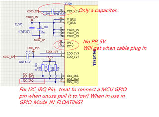
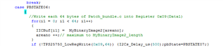
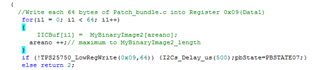
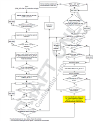
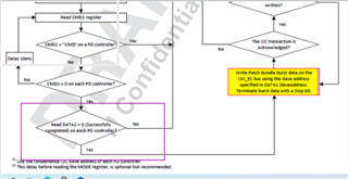
I cannot access the GUI. Otherwise, the bin file generated from GUI maybe un-useful for me, for I want to configure the PD controller via the I2Cs port with a MCU.

Could you please help to reply these questions below?

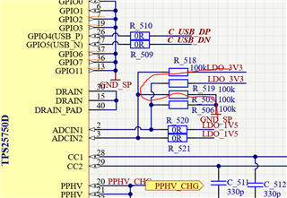
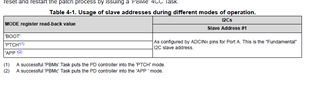
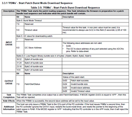
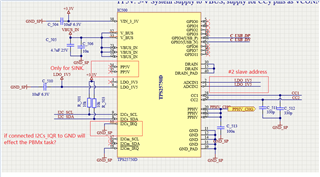
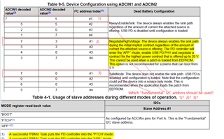
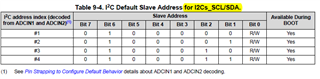
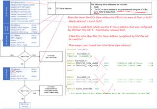
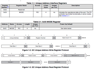
-  Is the Slave address, maybe one of #1,#2,#3,#4 which was configured from ADCIN1&ADCIN2, the Unique address?

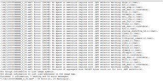
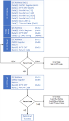
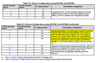
   So, the address in the register table(2-1) are the register numbers(Table 1-1). 

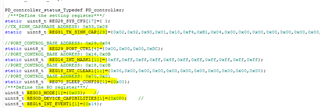
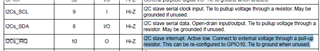
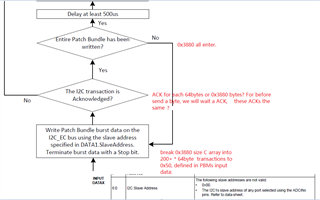
 -   The Engineer told me that it can take 1 of 4 I2C addresses, 0x20, 0x21, 0x22 or 0x23, as the slave address. But I found that it seems ignored the bit0(W/R)? For the bit0 cannot be sure from datasheet view, which decided by the actual condition.

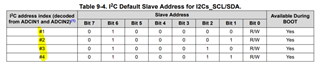
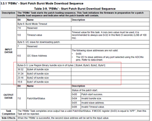
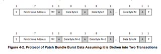
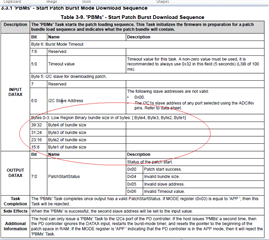
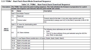
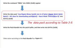
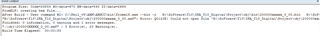
- The table below, where can be looked for? I cannot find in the datasheet and  also the technical reference manual, but it's really important and necessary for developers.

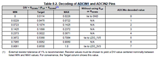
That's why I'm confused on the actual slave address, as well as the unique address. If have no these data, we really don't know how to configure, what’s the meaning of the decoded values, for there are 3 teams of configuration:

Thank you,

Franz

  • Hi Franz,

    Can you confirm which EVM GPN that the customer is using?

    This may be more of a question for the MSP430 team because it appears that you are trying to communicate with the MSP430 on the EVM.

    Thanks,

    Matt

  • Sorry, the IC is TPS25750, which i discribed no clearly.

    The slave address is clear.

    Thanks,

  • Is there anything I can do to help with this issue?

    I am from the TPS25750 Team.

    Regards,

    Chuck

  • Hi Chuck,

    Thank you very much.

    If we don't want to use the binary which created from GUI, for there are also additional components and programming steps, that also wasted more PCB space, as well as the produce time, which we really care.

    So if we want to configure the PD controller with EC, and develop configure software by ourselves, it's better to select another PD controller, right?

    Could you please recommend one from TI, which can meet our requirement?

    Thanks,

  • Matt,

    The boot and configure sequence is actually a very simple set of I2C commands, so any EC can easily program the TPS25750.  There is almost no performance requirement in the MCU, just an additional memory requirement.

    The TPS25750 has an pin strap option called AlwaysEnable5V that will ensure that a 5V contract is negotiated with up to 3A of current that will allow your system to boot.  The easiest way to configure this is to connected a resistive divider with 100K to LDO_3V3 and 100K to GND and the center node of the divider to ADCIN1 and ADCIN2.  I suggest 2 resistive dividers to allow you to change the I2C address or mode if you wish.

    Here are the base set of requirements 16kBytes of free memory for the boot and configure array (the current array is about 12.5K, but may grow with the standard, so we recommend supporting the full 16KB)  We provide documentation on the I2C commands that are used to boot the in our Technical Reference Manual.  Within the TRM there is a flowchart that is referred as the Patch Bundle Mode.  This will describe the commands you will use in your EC.

    Please reach out to me with any further questions.

    Regards,

    Chuck

  • Hi Chunk,

    Many thanks for reply.

    Right now, the slave address has been configured as the same as you suggested.

    My wondering is that, how to configure the PD controller.

    What I did right now is that, write the WR registor as soon as power on for the MCU.  

    The WR registers from the TRM as bellow, i set the bytes' values also refered to USB PD spe. 3.1, and have also tried several teams, but seems the PD controller has no response. Of course, the read write squences must strictly implement the I2Cs protocol of TPS25750.

    You mean when safe_5v is detected, configure the PD controller with the "4CC comands"? Don't need to write the WR registers to configure?

    If like this, you mean there are a default configure already, just need to change to what i want by send the "4CC conmands"?

    For example, change to power role to Sink, PDO to15V 3A.etc.

    could you please help to guide?

    I really don't know whats the key points.I asked many times in the past months, but there are really still no directly and clearly answers. All the answers let me wondering.


    1. Does the Binary file, which is created by GUI could it be replaced by writing the WR registers by EC?
    2. What are the contents of the Patch Bundle? What is the function of the Patch Bundle?
    3. When is the 4CC commands used? When does it work? Is it used in PD controller configuration?
    4. Could you please give a guideline for configure PD controller by EC? For users don’t want to use the costmized GUI tool  binary, as well as an EEPROM.

    But we wish to configure with EC directly.

    Thanks,

    Matt

  • In your schematic, you need to pull the I2Cm_IRQ pin high with a 10K ohm resistor in order to allow for interrupts to work.  Right now it will always assert the interrupt, which will require you to mask all interrupts in your configuration.

    You also do not need to supply PP5V in a sink only application and VIN_3V3 only needs a capacitor, not a connection to a LDO.

    In order to configure the TPS25750 using a MCU, you will need to generate a low region binary using our application configuration tool:  https://dev.ti.com/gallery/view/1769824/TPS25750_Application_Customization_Tool/  This tool will allow you to configure the device to meet your needs by answering the 10 basic questions and then select the advanced GUI to disable all of GPIO that are grounded.  

    I have highlighted the button you will need to click after you have answered the 

    Once you have the binary file generated, you will need to translate it into a c-array for your MCU to use with our PBM flow described in this document:  TPS25750 Host Interface Technical Reference Manual

  • Hi Chuck,

    Thanks a lot.

    - cerrected as below: Are the PP5V and 3.3V will be gotten from VBUS&VBUS_IN?

    -I open it by use Ultra Edit. A large QTY of data. Then  

    Then put the data(as hex data) according to the "Bytes 0-3: Low Region Binary bundle size in of bytes: [ Byte4, Byte3, Byte2, Byte1]"?

    And follow the Protocol of Patch Bundle. It will be rather  a very large C arry.

    i will define a c array as bellow show for sending the data.

    uint8_t pArray[ ]= {'byte1',--------,'byteM' }; //M is the number of thedata which translated from binary file. eg: pArray[0]='0x01' and so on.

    Is that right do like this? Please give some suggestion.

    Thanks,

    Matt

    Thanks,

    Matt

  • Matt,

    I have had a few customers report success using this flow:  https://www.keil.com/support/docs/4038.htmReading

    It makes the process more automated.

    Chuck

  • Hello Chuck,

    Thanks a lot, I have  generated a c source file and a included file for the configure from the GUI Tool.

    But i still have some questions:

    - I found the Unique Slave Address is 1# , as the content shown in TRM, is that mean when we updating a patch bundle, only can use 1# address?

    - As show below, the DATA1 is 64bytes , but Table 3-9. 'PBMs' - Start Patch Burst Download Sequence shows Byte0-3 are the Low Region Binary bundle size in of bytes. I'm wondering that, how many bytes shall i write one time? 64 bytes or 4 bytes?


    - Like shows in the Table 3-9, is that the format as bellow every time when i write into DATA1 Register? That means the patch bundle data will be loading with the other content every time. That mean each time there are only 4 bytes for Low Region Binary Data?

      Low Region Binary bundle size in of bytes: [ Byte4, Byte3, Byte2, Byte1]+I2C slave for downloading patch[Byte5]+ Burst Mode Timeout[Byte 6]

     What is the right understanding?

    Could you please give me some guiding, thanks.

    Thanks,

    Best Regards,

    Matt

  • Matt,

    The easy way to keep the I2C addresses straight is to follow this rule:

    The address that you write in the PBMs command is the address that you write the entire c-array to,  all other I2C writes go to the Cobra address (0x20 to 0x23) depending on the ADCIN1/2 settings.

    The Bundle size is the total number of bytes that you are going to write to the patch buffer, so it should be one of the numbers in your include file.

    I believe that you can write the entire Patch Bundle in one very long I2C transaction, but this will depend on your MCU.  You may have to chunk it into smaller writes so that you do not have issues with peripheral buffers.

    The timeout value is a watchdog timer that will end the process if you do not complete the patch within the target period.  The TRM recommends 5 seconds.  With very optimum code, you can load the entire patch in about 500mS.

    Please fee free to ask any additional questions that you may have.

    Regards,

    Chuck

  • Hi Chuck,

    Thank you for your quickly reply. To be a little bit specific:

    - For the I2C slave address: 1# is only the "Fundamental"  I2C slave address, so it's only the default I2C slave address as soon as power on and before PD controller read the ADCIN1/2 settings. The actual I2C slave address will be decided by the ADCIN1/2 settings. Could I understand like this?

    - For the implementing of INPUT DATAX, which be listed in "Table 3-9" : My question is on "Table 3-9", in which table they defined 6 bytes for INPUT DATAX, Is that mean before I write the Patch Bundle into the patch buffer, and then write into DATA1 (0x09), I also have to write the data pack "Low Region Binary bundle size in of bytes: [ Byte4, Byte3, Byte2, Byte1]+ I2C slave for downloading patch[Byte5] + Burst Mode Timeout[Byte 6]" into DATA1 (0x09)  as soon as i write the command "PBMs" into register CMD1 (0x08), right ?

    Is the operating flow steps correct? This is important for me to implement in software.

    Thanks!

    Best Regards,

    Matt

  • Matt,

    You need to write the PBMs command completely where you write the Data1 register as described and then write to the Command register 'PBMs' and then read back the Command register until it reads back zero.  This means that the command has been accepted.

    After this, you write the full patch into the patch register address that you set in byte 5 of the PBMs data.

    After this, you can then follow the rest of the flow.

    Regards,

    Chuck

  • Hi Chuck,

    Thanks,

    I'm not completely understood about how and where to use the "table3-9", I will try as follow for issue a "PBMs" task and feedback the result.

    Thanks,

    Matt

  • I am going to look at this in detail on Monday to get you a better response.

  • Matt,

    I am still looking at this.  

    Do you happen to have a TI sales or FAE contact?  This would help me with privately sharing your code with me for review if you have a contact to work with.

    Regards,

    Chuck

  • Hi Chuck,

    The C array is a very long one. ( project information:(keil, uvision5), MCU: stm32f103RCT6(48k SRAM, 256k flash))

    I write 64 bytes once from the C array to DATA1 buffer.

    When compile there are lots of errors:

    If comment it out the error will be disappeared. I think this was related the SRAM of  the MCU. 

    But for so large array, how to handle, could you please give me some guide?

    I think you can give me some ideas.Slight smile


             case PBSTATE06: 
                 {  
                   //Write each 64 bytes of Patch_bundle.c into Register 0x09(Data1)
                    for(i1 = 0; i1 < 64; i1++)
                    {
    //                  IICBuf[i1] =  MyBinaryImage2[areano];
                      areano ++;// maximum to MyBinaryImage2_length
                    }
                    if (!TPS25750_LowRegWrite(0x09,64)) {I2Cs_Delay_us(500);pbState=PBSTATE07;}
                    else return 2;
                 }
                 break;
             case PBSTATE07: 
                 {     
                    //Write PBMc command(“PBMc”(0x50424D63) into Register 0x08(Cmd1)
                    IICBuf[0] = 0x50;
                    IICBuf[1] = 0x42;
                    IICBuf[2] = 0x4D;
                    IICBuf[3] = 0x63;
                    if (!TPS25750_LowRegWrite(0x08,4)) pbState=PBSTATE08;
                    //Poling Register 0x08, it means success if 0x0000_0000,  it means fail if ”!CMD”
                 }
                 break;
              case PBSTATE08: 
                  { 
                    i1 = TPS25750_RegRead(0x08);//Read CMD1 register 
                    if (i1 == 0)
                      {
                        if ((IICBuf[0] == 0x21) && (IICBuf[1] == 0x43) && (IICBuf[2] == 0x4D) && (IICBuf[3] == 0x44)) pbState=PBSTATE10;
                        else if ((IICBuf[0] == 0) && (IICBuf[1] == 0) && (IICBuf[2] == 0) && (IICBuf[3] == 0))pbState=PBSTATE11;
                      }
                  }
                break;
               case PBSTATE09:  
                   {              
                     if (areano >= array_rng){I2Cs_Delay_us(500);pbState=PBSTATE07;}
                     else pbState=PBSTATE06;
                   }                
                 break;   
    

    Comment out

    Comment out

    Thanks,

    Matt

  • Matt,

    What is the status of your issue?

    Did breaking the array into smaller sub arrays allow you to proceed successfully?

    Chuck

  • Hi Chuck,

    The issue on Table3-9 still waiting for your reply.

    The compiled error is another one. Today I will try to find some special process on memory allocation, dynamic memory allocation or move the storage location for the C Array out of 48K SRAM .

    But i think maybe there are some relationship potentially, for i still don't know what's the usage of the 6 bytes for INPUTDATAX which were defined in table 3-9.

    How to use this table? When and where to use?This table may tell how to sub the patch bundle, how large the sub-package is. Right now, I did just refer to the ways someone did for TPS25798DHH.

    But it's not completely the same according to the TRM, but I don't know how to do so far.

    If these are right, the problem will be easier.

    Thanks,

    Best Regards,

    Matt

  • Hi Chuck,

    The above compiling errors were resolved. 

    Thanks,

    Matt

  • That's great to hear.

  • Are there some progress on the table-3-9  from your side?

    Thanks!

    Matt

  • Matt,

    I am working to see if I can share a section of a soon to be released update to our TRM that has a better description of the code you are working on.

    I will be out of the office tomorrow, so it will be next week before I can get back to you.

  • Hi Chuck,

    That should be great! Thanks a lot.

    Best Regards,

    Matt

  • Hi Matt,

    Thank you for your patience, Chuck will provide additional feedback next week.

    Thank you,

    Hari

  • Hi Chuck,

    Are there any news?

    Thanks,

    Best Regards,

    Matt

  • Matt,

    I have copied a flow chart from the next generation TRM that I hope is more clear.

    Are you stuck at the highlighted section or somewhere else in the process?

  • Hi Chuck,

    I just finished the code, and start debugging. If there are some progress or problems, i will feedback to you.

    Thanks,

    Matt

  • I'm happy to help.

  • Right now, the software canbe running according to the flowchart in TRM.

    But stuck at the step, which is marked at below purple square frame:

    The CMD1 register was 0000, but values of DATA1 are still "PBMs", i don't know why?

    Coud you give some advice?

    Thanks,

    Matt

  • Matt,

    I think I understand where your confusion is coming from.  I will work up a graphical representation of how a 4CC command works and I think this process gets a lot easier.

    The way the the flow works, you write the PMBC 4CC command, then transfer the bulk EEPROM, then write the BPMs and PBMe 4CC commands and the process is done.

    I will draw up a graphical representation of the 4CC command for you and then you can write a function to execute it and then this will get much easier.

    Regards,

    Chuck

  • Chuck,

    Good morning,

    Thanks a lot for your reply in due course of time.

    The R/W for the registers, INT_EVENT1, MODE, CMD1, DATA1, before this step are all right according to the flowchart.

    I think it's only one step away from realizing the function. I'm looking forward to and excited.

    Thanks,

    Best Regards,

    Matt

  • Hi Chuck,

    For the PCB is not a latest one not easy to correct the I2Cs_IRQ, which was connected to GND, as bellow shows, or to say if I connected the I2Cs_IRQ to GND, does it effect the PBMx task? When to use I2Cs_IRQ pin?

    Are there some internal relationship between these or not?

    According to the data sheet, in which seems "LOW" is active voltage level, that means if connected the GND, the PBMx task will be happen in time. I think we can connect the I2Cs_IRQ to GND directly, am I right?

    Thanks,

  • Hi Chuck,

    I saw the two points remark in the right down corner of the flowchart, which indicted to use fundamental I2C slave address, the #1 slave address.

    But in the TRM, there are 3 fundamental I2C slave addresses. I'm not sure which one is the right one

    Could you please give some suggestions?

    Thanks,

    Best Regards,

    Matt

  • Hi Chuck,

    See picture shows, could you please help to check the question? For the values of DATA1 were still 'PBMs' after CMD were all '0'. So the flow cannot be gone on. This is the problem right now. 

    I saw the TRM declare the PD controller will never modified the DATA1 value once CMD has changed to 0. Is that means the CMD was modified to 0 too early? That latched the values of DATA1 cannot be change to 0. Why the PD controller changed the CMD to 0 before modified DATA1 TO 0?

    I am wondering the root reason?

    Thanks,

    Matt

  • Matt,

    The 4CC commands are actually a string processor with a data phase and a command phase.  The figure below shows the progression on the PBMs 4CC command in a manner that I think is much more clear.

    The IHI I2C read and Write commands follow the standard I2C read and write format, and I have demarked the data flow and when to do reads and writes to execute the command.

  • Hi Chuck,

    This flow chart help me understand all the 4CC task table in the TRM.

    Thank you very much.

    Matt

  • Hi Chuck,

    It seems the slave address(including W/R bit) are:

    ----- Wr   /   Rd ------

    #1:  0x40 / 0x41                0x21<<1= 0x40        (0x21<<1) |1= 0x41

    #2:  0x42 / 0x43                 --------     

    #3:  0x44 / 0x45                 --------

    #4:  0x46 / 0x47                 ---------

    -----------------------

    Why bit0 is not included?

    For #2 : when write why not to send 0x40, when read why not to send 0x41 ?

     Am I misunderstanding?

    Right now, the PatchStatus bit for DATA1 is still 0x05.

    Wondering!

    Thanks,

    Matt

  • Hello Chuck,

    I have some questions on this chart, which were marked in the figure, could you please help to clarify.Thanks.

  • Sorry, the PatchStatus bit of PBMs data pack has been changed to 0 now. Waveform also right.

    I think my understanding is right.

    There need a delay between write PBMs to CMD1 and read DATA bit 0,

    So the slave address and issue PBMs question were resolved.

    Thanks,

  • Hi Chuck,

    In the next steps, could you please give some advice for the questions in the figure below.

    Thanks,

    Matt

  • Matt,

    The easiest way that I can describe the I2C addressing for the PBM flow is as follows.  The Device address that you use for the 4CC commands will always be 0x20-0x24 (zero out the R/W bit in most systems) depending on the setting of the ADCIN1/2.  The slave Address in the PBMc command cannot be the same address as the host interface (0x20-0x24)  This address is used as a bulk buffer to store the entire patch.  I usually suggest that customers use 0x50 because it is the EEPROM address and is very unlikely to be used in any system.

    To write the patch bundle, keep writing your 64 byte blocks into the I2C address that you selected in the PBMc command until you have written your entire block eeprom space.  This can be 100's of 64byte blocks.  It does not matter how many you use, as long as they all follow proper I2C protocol.

    After you have written the whole eeprom, then you will need to issue the last 2 4CC commands to finish your update.

  • Hi Chuck,

    Yes, i have written all the 0x3880 size of patch bundle data to 0x21(0x40), so as your suggestion i changed the slave address to 0x50 for PBMc task, the value of CMD register has been changed to 'PBMc', but it kept and never be changed to 'APP' any more.

    You said "After you have written the whole eeprom, then you will need to issue the last 2 4CC commands to finish your update."

    This were not shown in the flowchart, how to operate?

    You mean:

    --->  written the whole PATCH bundle(write to 0x21/ 0x09)--->PBMe(write to0x21/ 0x08)--->PBMc(write to 0x50)?

    the 2 4CC conmands are PBMe(write to0x21/ 0x08)--->PBMc(write to 0x50)?

    Thanks,

    Matt

  • MAtt,

    You need to write the PBMs command to 0x21

    The write the entire eeprom array to 0x50 (the i2c_addrress of the PBMc)

    Then write PBMc to 0x21 and then PMB to 0x21.

    This should complete the patch process.

  • Hi Chuck,

    Thanks,

    But i cann't find any information in TRM for 'PBM'task, i will try it.

    To write 'PBM' to 0x21 as soon as write 'PBMc' to 0x21 finished?

    Maybe there are some other problems. 

    Thanks,

    Matt

  • Hi Chuck,

    Where to write 'PBM', is it only a command?

    Thanks,

    Matt

  • Hi Chuck,

    When i use 0x50 for PATCH bundle loading. the PD controller cannot recognize this address.See picture shows.

    I've no idea now. Please help to analysis.

    Thanks,

    Matt

  • Matt,

    Here is the capture of the PBMc for your settings from my developers tool:

    This is the Data Write to the Data1 Reg

    This is the Data write to the CMD1 Reg

    I did not capture the to polling steps, but they run cleanly as well.