This thread has been locked.

If you have a related question, please click the "Ask a related question" button in the top right corner. The newly created question will be automatically linked to this question.

DRV8302: failure of drive chip when running.

Part Number: DRV8302
Other Parts Discussed in Thread: DRV8353

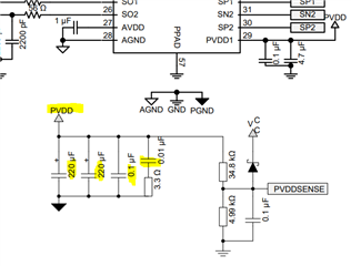
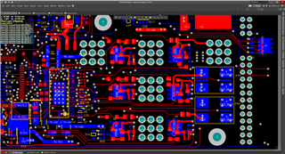
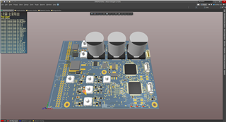
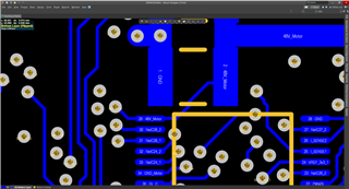
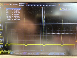
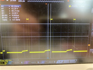
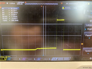
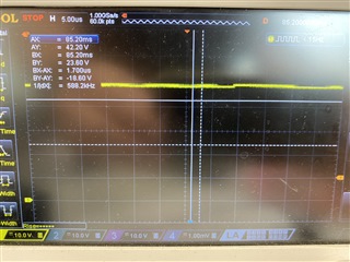
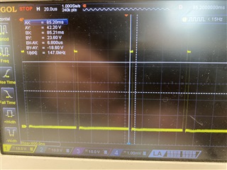
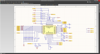
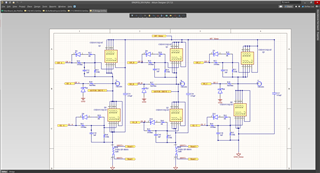
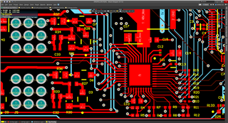
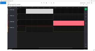
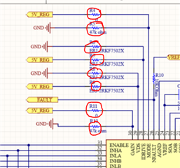
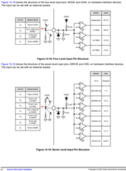
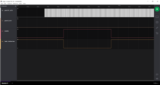
Currently in design / prototype we have 48 brushed motor design (with ability to go to 3 phase brushless ) We are seeing the same failure at 24v and at 48v. One of the failures is when we demand the motor to work then stop (energy still in system abrupt stop to go the other way ) The DRV8302 fails - the 5v stays up but it fails in such a way if i replace the chip its taken the PCB with it (6 layer , things are tight ). I do have a feeling I have a layout problem maybe some tracks need to be floods as I've looked at the design guide. The design guide shows for a 2 layer board , as I've said mine is 6 layer with a GND plain. We have also seen the track from 2.2uF caps to pin 29 blow (this could have been due to operator connecting a 48v inverter up to the board incorrectly) i am happy to post up Altium schematic and screen shots of layers / gerbers 

drv8302_screen_shot.docx

  • Hi John, 

    Thanks for posting your question to the e2e forum.

    We are looking into your inquiry and will follow up soon.

    Best Regards,

    Andrew

  • Hi John,

    Please see the below suggestions and questions in response to your e2e post: 

    Questions:

    1. what is your expected motor phase current during regular operation? and peak current expected under high load?
    2. Other than the situation described above where the motor is demanded to stop (brake/stall condition), does the motor system run fine normally? 
    3. Fault condition
      1. does nFAULT (pin6) pull low during this situation? 

    Suggestions:

    1. Bulk capacitance (page 24 of the datasheet, section 9.1 titled 'Bulk Capacitance')
      1. on the schematic provided, I am only seeing two 2.2uF caps and one 100nF cap for the PVDD1 pin.
      2. Situations like the forced brake/stop you mentioned will result in the motor pulling a lot of current from the 48V PVDD bus, cause it to change from 48V. 
        1. In this case, you need bulk caps in the system to provide this immediate current or else the 48V will drop and cause problems
        2. these missing caps might explain why your 2.2uF caps blowing during motor brake 
      3. In the datasheet page 21, section 8.2 for 'Typical Application' diagram - there are two 220uF caps which are for 'bulk' capacitance. 


    2. Layout
      1. It's hard to tell from the Altium layout screenshot alone, but the capacitors related to the DRV8302 device need to be placed as close as possible to the IC's pins. This typically includes caps such as: (between CP1 and CP2), for DVDD, for BOOST, and for PVDD1/PVDD2 bypass and bulk caps - to name a few. 
      2. also, gate drive traces (for signals like GHx, SHx, GLx) need to be ~15-20 mils thick so that the motor commutation signals don't have excessive noise/transients. 

    3. Attached the two links below that may be helpful to your system design, especially for layout.

    Documentation:

    Thanks and Best Regards,

    Andrew

  • the 3 caps are 1000uf each .. 

    the top two studs are 48v + top and 48v gnd underneath it ... on an inner layer the 48v joins to the stud in the middle of the board , the next screen shot is the board flipped in altium showing the drv chip 

  • Hi John,

    Thanks for the updated info -

    We will look into this further, and see if we have any additional suggestions to help resolve the problem.


    As for ongoing questions and info needed for debug, please see the two items below 

    1. would it be possible to probe the PVDD/PVDD1 waveforms, and also the SH_A/B/C waveforms, and share the screenshots here?
    2. what is expected motor current during normal operation and at peak loads?

    In the meantime, the two documents I linked will help advise on different options for improving your system's performance

    Thanks and Best Regards.

    Andrew

  • i'll get some photos / screenshots and upload 

  • Hi John,

    Also - as a secondary request - would it be possible to capture and share some info on the damage done to the DRV device?

    One way to do this would be to measure the resistance to GND for each pin on DRV8302 and identify any opens/shorts that are different from a non-damaged device. 

    Thanks and Best Regards,

    Andrew

  • ah blast i threw the damaged chips away ...

    but what i can tell you is that when the board take the "hit" the chip does pop and all h bridge drive stops (all the bridge is ok - as in no FETS are shorted ) but i still have all the buck / boost up and running as the logic circuit stays up. 2 of the chips i've had go they have 'cracked ' by pin 29 plus one blew the track going to it (but  

    After reading the links you have posted up on here i do think i have a lay out problem - i was a bit rushed as we needed something for the software guys to use ...

    The project is done under altium. If you have access to Altium and would like a look at the PCB layout , i'm fairly sure i can let you have a copy or even if we discuss it over "teams " with screen share.  I have been thrown in at the deep end with this. I did lay most of the board out (just not the drive stage ) but we used the chip in a previous project but at 12v with no grief and i did didn't even think we'd have problems " as we've used it before with no problem". 

  • waveforms ... as asked for these are up at 48v ... the scope is set 10v per div. 

    this is SH-A ... note how the spike is at nearly 58v..

    SH-B , maybe with motor going other way.

    a zoomed in of the above - again spike is close to 60v 

    this is quite close to the PVDD pin 29 of the chip 

    this is a caputure of one of the h- bridge lines going to the motor - i plan to clamp these with some zener diodes as a trial. The motor is barely being asked to do anything here and I've got 56-58v spikes ( well it is a motor .. ) so i would expect these to be a lot higher the more effort the car is being asked to do.

  • Hi John,

    Thanks for your updated response - the inclusion of the waveforms and the description of the failure mode reported are very helpful.
    Based on this latest information, I do have some updated feedback for you - please see below:

    1. We understand that your system's nominal operating voltage is 48V.  
      1. the DRV8302 device is only a 60V part with an abs max rating of 65V, so it may not be appropriate for 48V. 
      2. we typically advise to select a part that is rated for 2x the voltage of your application, to handle transients like shown in your waveform.
      3. Question: what is your expected motor output phase current? this detail is important to know if DRV8302 can be used for your 48V application. 
      4. Question: I saw that your initial post mentioned the 24V nominal voltage case also having failures. Is this true?
        1. What is the need-case of your system design? If 24V is acceptable, then DRV8302 can still be used
          1. we would need some similar information like PVDD1/2 and SHx waveforms, this time for 24V, to help debug the system

    2. In the case where 48V is still needed in a high-current application, it may be necessary to redesign the system using a similar part
      1. for 48V, we advise using the 100V-rated part: https://www.ti.com/product/DRV8353. Table 5 in the datasheet will explain the part names 
      2. Specifically, the part name to order within this product family that would match your DRV8302 closely is 'DRV8353RH' in a 48-pin RGZ package. 
      3. this part has many of the same features you're using, such as:
        1. 3x current shunt amplifiers, integrated buck regulator, 6x PWM input control logic, fault detection, and various regulators for internal device operation as well as external voltage bias. 
      4. some notable differences are: 
        1. DRV8353RH uses a charge pump architecture, instead of the DRV8302's bootstrap+trickle-chargepump design 
        2. DRV8353RS is a SPI-enabled version that gives you more control on things like fault reporting 
        3. DRV835x family has less source/sink current (1A/2A) capability than DRV8302 (1.7A/2.3A), but 1A/2A may be sufficient for your application based on MOSFET Qgd spec and your intended switching freq and rise time 

    3. Lastly, regarding a schematic and layout review - 
      1. our team is available to help review schematics and layout, so if you have a new design and want to ask for advice over a meeting or an email, just let us know and we'll support it accordingly 
      2. in the meantime, those two documents on layout and board design can help you and your team identify changes needed
        1. design choices like mentioned below can help reduce the severity of transients/spikes that you're seeing on SHx and PVDD
          1. placing bulk/bypass caps close to the MOSFETs
          2. having 15-20mil thick gate-drive traces 
          3. proper routing of high-power traces of MOSFETs power-stage and having a proper return path for current on ground plane
      3. i've reattached them here + added a new link to help your research
        1. Board Layout Best Practices: https://www.ti.com/lit/an/slva959a/slva959a.pdf?ts=1631161865508
        2. High Power Motor Driver system design: https://www.ti.com/lit/an/slvaf66/slvaf66.pdf?ts=1631161862767
        3. Smart Gate Drive app note: https://www.ti.com/lit/an/slva714d/slva714d.pdf

    Thanks and Best Regards,
    Andrew

  • After discussion with the powers at be the plan is to order DRV8353HMRTAT ( because that is what i can get hold of at the moment ) - enlarge the board and turn it in to a dev. pcb so we can make sure we a) understand the hardware b) the software guys can continue with there work.

    Once i've relaid the PCB for the 100v part - who do i contact for help / advice / check i've not done something stupid - as you said earlier ..

    When i said to my colleagues that i'd had a detailed response from your selves they was extremely impressed - keep it up , just wish other manufactures did this and replied so well  :)

    Many thanks for the replies 

  • Hi John,

    Thanks for the update, and appreciated on the kind feedback! We are happy to help. 

    As for the sample ordering, the DRV8353HMRTAT does not have an integrated buck regulator feature.
    You'd have to have another external buck regulator IC on the PCB. Would this be acceptable for your application during development? 

    If integrated shunt amplifiers and integrated BUCK are a necessity, then DRV8353RH would be the right part for that.

    • I can talk to a team member to see if we can support small-qty sampling of DRV8353RH.
    • How many samples would you need? Would something like ~10pcs be sufficient for your early development? 

    Also, one quick clarification: I previously mentioned 48-pin RTA package, but it is actually a 48-pin RGZ package. My apologies for the confusion

    • the 'R' in DRV8353RHRGZR stands for 'integrated buck regulator' in this case

    For your second question on who to contact for help/advice with the new PCB system redesign, please feel free to make a new forum post or click the 'ask a related question' button on this post. It will get assigned to one of our team members.

    Best Regards,
    Andrew

  • Hi John,

    Following up on this discussion - 

    Please help answer the questions below on your sampling needs within the DRV835x device family. 

    I confirmed with our product marketing team today that we have 5 samples of DRV8353RHRGZT ready for shipment.

    • Please let me know if you would like to proceed with this option
    • I would need some information from you such as full shipping address and contact information

    Best Regards,
    Andrew

  • yes please . It would be handy as an option.. I have re-laid the PCB out with the none - regulator built in as i had to do something quickly and i've picked a regulator and added that aswell 

    Would you like me to private message you our address ?

  • Hi John,

    Thanks for the update, and sure - that would work.

    Please send me a private message with the full contact info and address (enough to fill in the user input fields below) 

    I'll follow up accordingly with our team to have the samples shipped 

    Best Regards,

    Andrew

  • PCB's are here , we are populating a small batch with pick n place. and i'll be testing very soon .. i will update here 

  • right , as it stands i cannot get anything out from the drive chip i've set just one PWM up to see if i get a response from a half bridge.  I'm set up as 6*pwm mode pin to agnd 

    and i've got my pwm out of dspic as complimentary pair and the drive chip just sets the fault pin low and ALL of the GL_? are on ..

    the motor is brushed so i'm using 4 of the gate drives.. 

  • Hi John,

    Thanks for reaching out again on this - we shall look into it and see if we can propose some solutions here. 

    To make sure we're aligned on the same info, can you confirm the following: 

    1. which part are you using at the moment? 
      1. is it the DRV8353HMRTAT (without integrated BUCK) at the moment?
      2. or is it the new set of DRV8353RHRGZT samples we provided a few units of? 
    2. is the latest schematic you sent me via private message up-to-date? 
      1. (i believe that one was for the 'M' version DRV8353HMRTAT) 

    Also, any other information you can tell me about your operating conditions or system behaviors observed will definitely help the debug process

    Best Regards,
    Andrew 

  • I am using the 'M' version without the regulator , i have external reg on the board

    resistors are set up for middle setting for gate charge and the gain of op-amps.

    with the chip enabled and no PWM's going in all inputs are LOW ..

    i'm open loaded ( brushed motor sits between motor drive 1 and motor drive 2 of h- bridge ).  I've left the h-bridge alone from when we used the drv8302 - i understand there is more protection in the 8353.. i can always take stuff off the board and jumper resistors.

    i'm testing at 12v with current limit low on power supply 

     VM is at 12v for now (VM and Vdrain are connected and will eventually be 48v)

    VGLS is 12v - - - i did find this not connected at the chip this has now been corrected 

    CPL has high frequency pulses small duty cycle

    CPH has same as above but on top of 12v 

    DVDD is 5v.

    GL_A , GL_B, CL_C are all at 7v which also means that they are all on - confirmed by continuity of motor drive to ground 

    nfault is low ... 

    I also have 2 PCB's exactly the same....

    following the truth table either the 6 pwm or the 3 pwm ... if all inputs are off then the all the gates should be low, its like its "braking" the motor

    Again this forum has really impressed me with the response , again if you can assist i'd be most gratefull

  • Hi John,

    Thanks for reaching out on this and providing the info -> i'll take some time to review this info today/tomorrow and will see if I have some additional suggestions on what the problem might be

    Best Regards,
    Andrew

  • looks like the chip is was damaged , i've built 4 boards up  now and the others are kind of awake. They dont follow the truth table so i'm a tad puzzeled at what to do next , i can set up waveforms to 'fire my h-bridge (i'm only down at 100hz at the moment as i'm unloaded and open circuit ) i do see the drive chip come out of fault when the piece of code is running but the bridge / chip doesnt respond correctly 


    pwm1high is on in1h

    pwm1low is on in1L

    pwm2high is on in2h

    pwm2low is on in2l

    from that the bridge should ( if i had something connected) spin a motor one way then the other - 

    all i really see is both half bridges go live , switch off then go live again .

    i'm set in independant mode / 6 PWM  but i'm going to try and set it in 3pwm mode and change my test code and see what the results are (i also have not seen any fast swicthing of ant FETS yet )

    progress but strange... 

    I'm happy to start a different thread as this is now a set up problem for the drive chip , if the moderators see fit 

    thanks

  • Hi John,

    Thanks for the additional information, and my apologies for the delay in my response - 

    I'll try to get you an answer on items reviewed by end of today.

    Thanks and Best Regards,
    Andrew

  • Hi John,

    Thanks for your patience - I have some feedback for you as promised, and let's see if we can get this system working again w/ the new DRV835x device. 

    Please let me know if the below information helps explain the situation well 

    Questions: 

    1. For the HW interface config connections (pictured below), are all of these connected at the same time? or do you depopulate one during checkout? see below comments on explanation for how to configure this (only one setting should be selected for each at a time) 
    2. what is the voltage you're seeing on VCP pin? 
    3. are you seeing the correct voltage on VGLS pin now?

    Observations/comments

    • on waveforms and signals:
      • DVDD measuring 5V is good, means the DVDD regulator is working 
      • CPH/L having high freq pulses is good, means charge pump regulator is working
      • VCP pin should be 10V higher than Vdrain when VM=12V, meaning it should measure ~22V. Can you confirm this?
      • VGLS pin should be ~11V when VM=12V. Saw mention that this was not set up earlier. Can you confirm if this is working now?
      • if your nFAULT pin is pulled low during a fault, this means the gate driver outputs will most likely be disabled/Hi-Z/floating 
        • first you have to get the device to exit the fault condition (by figuring out what type of fault is occurring)
        • (see table 13-6 Fault Action and Response) for each fault type 
        • only then will you be able to use the gate driver to toggle outputs using PWM inputs (this is true for any PWM mode) 
      • Figuring out what fault is occurring
        • if all 4 of the regulator voltages above are working while nFAULT is low, then that helps eliminate the possibility of all 4 'undervoltage' type faults (VM, VDR, VCP, VGLS) 
        • if device isn't really operating, then it's unlikely that it would be an over-temperature fault (OTW, OTSD) 
        • it is possible that we are experiencing either type of overcurrent protection fault (VDS_OCP and SEN_OCP) 
        • it is also possible that we have a gate driver fault (GDF), which happens when you apply signals on inputs INx and don't see a resulting change on the gate driver output pins (GHx, GLx) 

    • on the schematic provided:
      • I am seeing a lot of connections for the 4 hardware interface pins, but am not sure what is populated 
        • you should be using only one setting at a time, meaning that one of these resistors has to be removed in your system.
        • the resistor you choose to disconnect will depend on what you want to do (see screenshot below, or datasheet page32) 
      • here's an example: for the DRV device's MODE pin, it can choose between Independent, 1xPWM, 3xPWM, 6xPWM modes
        • if you want 6xPWM mode, you need to tie the MODE pin to AGND. (4th row on page32 tables for STATE/RESISTANCE/MODE/GAIN)  
          • this means you need to replace R5 with a 0-Ohm resistor, so that it's a direct short to GND
          • you will also need to completely remove R4 in this case, so that the device doesn't get connected to '5V_REG' which I suppose is DVDD. 
        • if you want Independent PWM mode, you will need to tie the MODE pin to DVDD directly 
          • this would mean keeping a 0-Ohm resistor on R4 to connect MODE to 5V_VREG/DVDD
          • you will also need to completely remove R5 in this case, so that there's no connection of the MODE pin to GND through any resistance 

      • the example above applies for the other HW interface features as well
        • your GAIN can be 5/10/20/40 V/V for the current shunt amplifiers 
          • this is for the motor phase current monitoring -> see the math equation in section '13.3.4.1 Bidirectional Current Sense Operation.' If you are using the wrong combination of gain, Rsense, and Vref -> this could trigger a Vsense overcurrent fault (SEN_OCP) & pull the nFAULT pin low, disabling the device because it thinks your motor phase has too much current
        •  IDRIVE setting controls how fast you switch the MOSFET gates on.
          • Too much causes ringing at switch nodes, too little results in inability to drive the MOSFETs (or very slow turn-on) 
        • Vds is another protection for overcurrent.
          • It's basically calculating how much current is flowing across the MOSFET, based on your MOSFET Rdson and the voltage drop between drain/source nodes (V=I*R).
          • If your Vds setting is too low, then it will trip overcurrent even though not that much current is flowing through the MOSFETs 
          • your resistor settings on Vds, depending on which one you populate, will have Vds threshold at either 0.7V or 0.2V (is this ok for your MOSFET Rdson and expected motor current?)

    HW interface configuration resistors (MODE, GAIN, IDRIVE, VDS) 

    Datasheet page32, shows info on how the HW interface pins (MODE, GAIN, IDRIVE, VDS) are set up and what bias settings correspond to what device behavior: 

    Best Regards,
    Andrew

  • Please be aware , I have mentioned this before. I am using a "brushed " motor , this is NOT connected to a 3-phase motor. I am using 2 of the half bridges.. 

    The hardware interface connections are only one at a time .. the schematic was just so I could get some 'pads' down ..

    The motor is currently not connected - i'm not going to connect anything until i see the 'bridge ' right.

    currently i have my R5 is 0ohm/shorted for 6 PWM (i have tried all modes) , R9 is 0ohm /shorted - disable vds ,  R12 is shorted - lowest setting as not calculated .

    • DVDD measuring 5V is good, means the DVDD regulator is working , ..... YES still ok 
    • CPH/L having high freq pulses is good, means charge pump regulator is working.... YES confirm still ok 
    • VCP pin should be 10V higher than Vdrain when VM=12V, meaning it should measure ~22V. Can you confirm this?  YES confirmed 
    • VGLS pin should be ~11V when VM=12V. Saw mention that this was not set up earlier. Can you confirm if this is working now? .. its nearer 12v ?

    I can see on layout is that i'm using a ground plane not ground flood and on your example layout the thermal pad is connected to your flood.. but as the chip wont come out of fault i cant tell if its going to over heat - the board is a dev item so if this needs addressing it can be done.

    wave form... 

    from the truth table , in 6 PWM this should trigger the GH_A, and as u can see as soon as i enable the chip ,i receive a fault.  At the same time GH_A and GH_B go high (12v) .. which means both sides of output to motor are live (i'm still open circuit) but also my unused half bridge GL_C goes to 7V so switching the FET on.. the other PWM's from my PIC are off. When Enabled the I_sense outputs are at 2.5v..

  • after some searching i found this..

    DRV8353: The gate driver does not work. FAULT condition all times - Motor drivers forum - Motor drivers - TI E2E support forums

    turns out if u don't have all three current shunts connected .. the drive chip goes in to fault ... 

    so after shorting out the 3rd current shunt i have this Slight smile

    i'd say this is a breakthrough

    the gates arent switching but i think it might be that i'm down at 100hz range ?

    i think i can go back to setting up the h-bridge at a high frequency ... unsure .. more playing er testing needed 

  • Hi John,

    Thanks for the update, and also for investigating this issue further through the other e2e forum posts.

    The resolution described makes sense for this situation, and we are glad that the nFAULT condition has been cleared! 

    • We will keep this suggestion in mind for future debug efforts on e2e, especially for customers not using all 3 phases with this device. 
    • To help close the loop on this discussion item about nFAULT specifically, we can conclude that the phase C shunt inputs (SPC, SNC) being left floating were probably causing a Vds overcurrent type of fault being reported 

    For the next step of your debug, I do have another suggestion: 

    • if the gates are not switching, it may be necessary to check the IDRIVE setting, and possibly increase it if needed  
      • it should be high enough to toggle the MOSFET gates at the needed switching speed 
      • once the switching is confirmed working, then next step is to tune the settings and eliminate 'ringing/transients' on the switch node
    • your other comment about 100Hz, and experimenting with the different settings may also be valid. Will have to experiment to find out 

      Looking forward to more updates on your progress!

      Thanks and Best Regards,
      Andrew 

    • and just to confuse matters..

      i wrote some code so i could test the board with the old chip (drv8302) i basically set all 6 pwm's going at 10% so i could test the h-bridge , the high /low was set to complementary again at 100%. just for interest i loaded it in to the new board with drv8553....All 3 half bridges are working but the nfault line is low which is strange.  I'm now going to do some testing by where i turn off the un-used half bridge to see if it still works and i can get a brushed motor to do something (or at least a sudo load / double led )

    • Hi John,

      thanks for the update - will keep an eye out for any follow-up messages here 

      Best Regards,
      Andrew

    • Ok.. 

      First things first ... Many thanks for the help from the forum and your self Andrew with out your suggestions of a chip change I would have been a bit unsure.

      As it stands today I've had a brushed motor spinning and quite high duty cycle ( @ 16Khz ) plus we have had the dev. kit being used properly in anger as it were up at 48v.

      i've tried running the motor off the h-bridge in 2 ways ..

      a) high side on the one half bridge PWM , low side GND on the half bridge

      and

      b) high side on one half bridge PWM but with low side complementary running as well ( with 100ns dead time so no shoot through) , then as above the other half bridge GND 

      I'm seeing better control with option b) and i can run higher duty cycle before the bridge / drive chip gives up and stops working.

      Even though i have not changed the bridge circuit (which is up above in this thread ),  I have (from your layout suggestions) used thicker tracks to the bridge from the drive chip. I've notice on the 'scope there appears to be little or no "ringing" , I have very close to a very good square wave on the motor (with option b) 

      I will try and get some photos up of wave forms across the motor of both options to show the difference from above with the drv8302

      At the moment my only addition i need to do is add the thermal pad to the ground layer - i'll probably do a small flood round the chip and use vias to join to my ground plane

      Again ... thanks for the assistance 

    • Hi John,

      Thanks for the update - in this case, we are once again glad to see that the new system is performing well!

      • Clean square waves are definitely a good sign, and the thick gate driver signal traces played a big role in that outcome 

      Pertaining to thermal performance, once again posting these two documents that may help your design - 

      https://www.ti.com/lit/an/slva959b/slva959b.pdf (Board Layout) 

      https://www.ti.com/lit/an/slvaf66/slvaf66.pdf (High-power system design) 

      Best Regards,

      Andrew