This thread has been locked.

If you have a related question, please click the "Ask a related question" button in the top right corner. The newly created question will be automatically linked to this question.

DRV8432: DRV8432 no output

Part Number: DRV8432

hi,

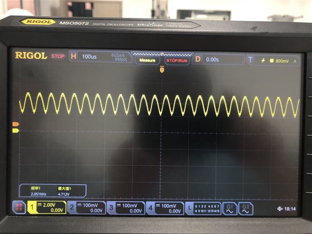
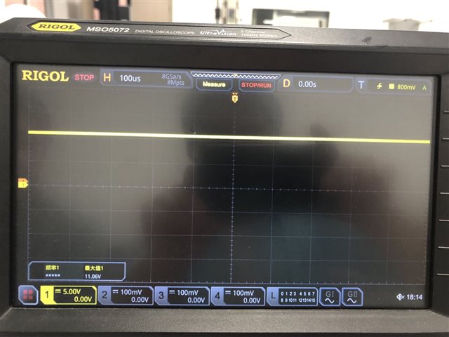
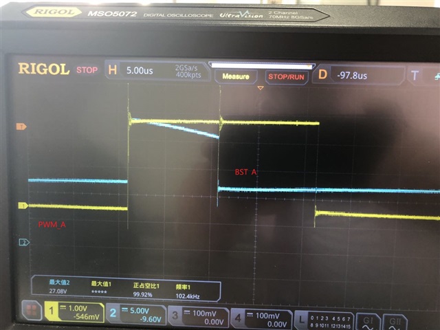
I'm using DRV8432 to drive TEC-XLT2418, but when giving PWM_A----10Hz 50% duty cycle PWM signal, PWM_B---Low, 

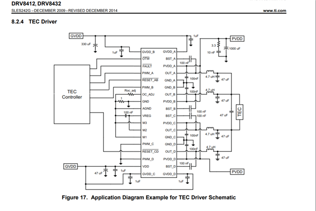
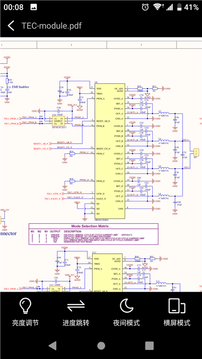
however, I can't get output signal for OUT_A, OUT_B, the design is below, please help check.

TEC module.pdf

BR
Jerry

  • hi team,

    I set up PWM_A 50% duty cycle PWM@20KHz, PWM_B low, RESET_AB and RESET_CD high, I can get output for OUT_A/OUT_B/OUT_C/OUT_D, but it's strange, at first, the OUT_A and OUT_B is sine waveform, and then always high---about 11.06V , so do OUT_C and OUT_D, waveform is below.

    could you help check,is it normal, why PWM_B can't control the OUT_C and OUT_D in mode 3?

    how to set up the control signal(PWM_A,PWM_B,RESET_AB,RESET_CD) for output signal we want to control TEC heating and cooling?

    BR

    Jerry

  • Hello Jerry, 

    I am happy to help out. Mode 3 is parallel mode which follows the following specifications per section 7.4 of the datasheet:

    In parallel full bridge mode (mode 3), PWM_A controls both half bridges A and B, and PWM_B controls both half bridges C and D, while PWM_C and PWM_D pins are not used (recommended to connect to ground). Bridges A and B are synchronized internally (even during CBC), and so are bridges C and D. OUT_A and OUT_B should be connected together and OUT_C and OUT_D should be connected together after the output inductor or ferrite bead. If RESET_AB or RESET_CD are low, all four outputs become high-impedance. Figure 15 shows an example of parallel full bridge mode connection.

    I have the following questions and comments that might be beneficial diagnosing what is going on:

    -Are you saying that you are providing a waveform for PWM_A at 50% duty cycle and OUT_A,OUT_B only follows it for a brief moment? If so:

    -How long can you provide a signal before the output latches high?

    -Would you be able to provide simultaneous scope shots of PWM_A, and OUT_A,OUT_B

    Would you mind sending a picture of your schematic to make sure that the device is set up properly in parallel mode? 

    Here is the datasheet recommended schematic for driving a TEC, I would check your design against this and try to make sure that it matches were possible. 

    Please let me know if you have any questions or if the recommendations provided did not resolve the problem. 

    Best,

    Pedro Arango Ramirez

  • Hi pedro,

    The schematic is below, I also uploaded the complete one, please refer to it, 

    How long can you provide a signal before the output latches high?

    ------ I always send 20khz 50% duty cycle square wave to pwm_a, set up pwm_b low,

  • Hello Jerry,

    Thank you for the schematic I will review it to make sure everything is in order. In the meantime, would you to care to elaborate on the other points listed above. Specifically, would you be able to expand on the following part of your post:

    "it's strange, at first, the OUT_A and OUT_B is sine waveform, and then always high---about 11.06V , so do OUT_C and OUT_D, waveform is below."

    Do you mean that at first the outputs match the sinusoidal input and stop doing so after a while latching into high? If so how long do they follow the input before latching high. And are there any faults reported when this happen. Would you be able to provide scope shots that have both the input and output in the same shot?

    Best,


    Pedro

  • hi Pedro,

    the scope shot of PWM_A and OUT_A is below, I also captured the PWM_A and BST_A,I found that BST_A would drop down within PWM_A high.

    please refer to that.

    BR

    Jerry

  • Hi Jerry,

    Thank you for the scope shots. I am a bit confused, it seems that the output voltage is incredibly low considering that GVDD is 12V per your schematic. This raise 

    In order to make sure that assist you as thoroughly as possible I want to confirm understanding of the problem you are experiencing:

    • Is the device operating as intended, managing to physically cool or heat? 
      • If it is not operating as intended, what is happening to OUT_A, is it latching high as per the first image?
        • Are there any fault notifications via the FAULT pin and OTW when this happens?
    • Are you able to use both heating and cooling?
      • One mode should be PWM_A oscillating and PWM_B low. The other mode should be PWM_A low and PWM_B oscillating. It is my understanding that only PWM_A oscillating and PWM_B low is working in your setup, is this correct?
    • What is the current going through the TEC on startup, and during operation?
      • It would be great to have a scope shot of PWM_A, OUT_A, OUT_C and current through TEC all in one scope, while keeping PWM_B low. This would allow us to better see where the problem is originating. 

    As per the second image you shared, I believe that could be an indication of bootstrap capacitor Under voltage Protection. There is a detailed explanation of this function in section 7.3.2.1 of the data sheet. 

    I apologize for not asking these thorough questions sooner, as I should've made sure that the problem in question is clear. I am always happy to help. 

    Best,
    Pedro Arango Ramirez

    PS: When reviewing your schematic I noticed that R30 has a value of 22kOhms. Because you are using the device in parallel mode you only have cycle by cycle current protection. It is not recommended to use such values in anything outside OC Latching mode per Table 2 of section 7.3.2.2 of the datasheet:

    hi Pedro,

    Thanks for your reply, I found the BST_X signal had a 100KHz frequency, so I have tried to set up PWM_X signal frequency 100KHz same as BST_X signal , see the waveform above,  it can solve the problem, but I don't know why that can solve, could you help analyze the reason why PWM_X's frequency should be same as BST_X's, or can we set up PWM_X signal frequency > BST_X's?

    about the R30,it's not recommeded to use 22K, so what's the recommended value for our 14A load?

    BR

    Jerry

  • Hi Jerry!

    I'm glad to hear that raising the PWM signal frequency fixed the problem. Looking at the previous waveform, and with your description of the solution I believe I might have an explanation of why the fix works. I believe it has to do with the Bootstrap capacitor Undervoltage protection. Information from the datasheet:

    7.3.2.1 Bootstrap Capacitor Undervoltage Protection When the device runs at a low switching frequency (for example, less than 10 kHz with a 100-nF bootstrap capacitor), the bootstrap capacitor voltage might not be able to maintain a proper voltage level for the high-side gate driver. A bootstrap capacitor undervoltage protection circuit (BST_UVP) will prevent potential failure of the high-side MOSFET. When the voltage on the bootstrap capacitors is less than the required value for safe operation, the DRV841x2 will initiate bootstrap capacitor recharge sequences (turn off high side FET for a short period) until the bootstrap capacitors are properly charged for safe operation. This function may also be activated when PWM duty cycle is too high (for example, less than 20 ns off time at 10 kHz). Note that bootstrap capacitor might not be able to be charged if no load or extremely light load is presented at output during BST_UVP operation, so it is recommended to turn on the low side FET for at least 50 ns for each PWM cycle to avoid BST_UVP operation if possible. For applications with lower than 10-kHz switching frequency and not to trigger BST_UVP protection, a larger bootstrap capacitor can be used (for example, 1-µF capacitor for 800-Hz operation). When using a bootstrap cap larger than 220 nF, it is recommended to add 5-Ω resistors between 12-V GVDD power supply and GVDD_X pins to limit the inrush current on the internal bootstrap circuitry.

    By raising the PWM frequency you allowed for the capacitor not to discharge fully and fully operate as intended. There are some fixes that you can do if you want to lower the PWM frequency like increasing the size of the capacitor per the guidelines above. 

    As for the resistor value for overcurrent protection.

    The table above pertains to the resistor value that determines the current per half bridge. Because you are running parallel current mode that means that for an overall current of 14amps, each half bridge will experience 7 amps of current. Therefore you should choose the resistor that is half the size of the overall current you desired. If you want an overcurrent protection system that kicks in at 14 amps, then you should choose a resistor between the values of 36-39 kOhms, such that the overcurrent threshold current in any given half bridge is between the 7.4 and 6.9.

    Always happy to help,

    Pedro Arango Ramirez