This thread has been locked.

If you have a related question, please click the "Ask a related question" button in the top right corner. The newly created question will be automatically linked to this question.

DRV8353R: Gate driver showing GDUV and UVLO faults

Part Number: DRV8353R
Other Parts Discussed in Thread: TPS54360B

Hi,

We are testing our custom hardware that used the DRV8353RS controlled by an STM32.

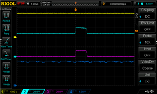
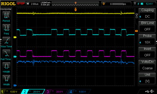
The main fault that we are getting is UVLO and GDUV, these occur at the same time.

The conditions for this happening seem to be high speed and about 20-30A load.

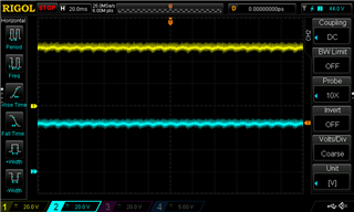
We are using fets with a Qgd of 34nC and an IDRIVE of 350mA. This ha been tested significantly on o controlled rig and the waveforms seem to be good, with almost no ringing at 15A (the maximum load we could apply) and temperature increase was acceptable.

It seems strange that we would be seeing these two faults as we are using a 48V battery (testing has been done between 42 and 48V) and VM is 12V supplied by a TPS54360B (so should supply 12V down to at least 20V).

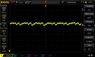
We have significant bulk capacitance (2 x 330uF), and capacitance on the 12V line (47uF electrolytic , plus 10uf and 100nF close to the DRV) so I would expect that a large voltage drop is not likely

Is there anything that we could try to eliminate this fault from occurring?

  • Hi Oliver, 

    Please see below feedback on your discussion items: 

    1. UVLO and GDUV fault presence 
      1. it makes sense that if your VM/Vdrain UVLO triggers due to a real fault, then it would understandably impact the device's HS and LS driver gate-drive-voltage sources, trigger a GDUV fault as a consequence (this would be the charge pump VCP and the other regulator VGLS, since they depend on the DRV device's VM supply source), 
      2. as for what's triggering these UVLO conditions exactly, 
    2. MOSFET Qgd and IDRIVE parameters
      1. given a Qgd of 34nC and IDRIVE of 350mA, I think this corresponds to about a 97nanosec rise time if my calculations are correct
      2. this is a bit closer on the aggressive end for MOSFET gate timing, but if you are not seeing ringing on the switch nodes then it should be okay 
    3. Bulk capacitance
      1. yes, 2x 330uF does seem like a healthy amount of capacitance - and the other caps mentioned sound reasonable as well
      2. still, since there is a UVLO fault triggering on VM or Vdrain -> need to confirm which one and then determine whether they're not being supplied enough current 

    Questions to help debug: 

    • does this GDUV and UVLO fault only occur under motor operation? 
      • or does it happen immediately at system power-up without MOSFET switching or motor being connected)? 
    • can you share some scope capture waveforms of the below signals? We need to confirm exactly which voltages are dipping below their UVLO thresholds to confirm if the various undervoltage faults are real and understand the timing of the problem 
      • signals: VM, Vdrain, VCP, CPH/CPL, VGLS  
    • can you try lowering the IDRIVE setting to see if at least the GDUV fault will stop happening? 
      • if GDUV is just a consequence of VM_UVLO, then that makes sense
      • alternatively it could be a possibility that there is also too much gate drive current being drawn for what the VCP or VGLS can supply, and that would be a separate independent root cause for GDUV happening 

    Thanks and Best Regards,
    Andrew 

  • Hi Oliver,

    Also one other thing - the performance of your battery management system in supplying power to both the DRV device and the MOSFET power stage VDRAIN bus is somewhat dependent on the layout of your PCB for these high-power signals, as well as how close your placing critical external components to the DRV device's pins. 

    • For the first suggestion about high-power signals, I've attached two resources below to reference what an ideal layout would look like
      • this would be some app notes, as well as the TI EVM specifically designed for this device 
    • For the second suggestion about capacitance, the resources will help as well 
      • but mainly this would be wanting to place caps for VGLS, VCP, CPH/L on the same layer as the DRV device, with proper thick traces (15-20 mils), close to the device, and to do as much as possible to avoid parasitic inductance as this would reduce the effectiveness of the caps 
      • also need to make sure the caps are properly rated for 2x their expected voltage (see component ratings on EVM design files for reference) to avoid DC de-rating and temperature de-rating 

    Resources:

    Best Regards,
    Andrew

  • Hi Andrew,

    Thanks for your response.

    The error only occurs when the motor is in operation. More specifically, this is for a small electric vehicle application, and the error occurs when the motor is spinning at about 500rpm and travelling at roughly 25kph with a rider on it. Our logs show that this is about 30A of load. This makes it difficult to attach a scope to it and monitor the lines that you asked for.

    When measuring this on a rig, we can spin to the same speed, but only apply about 15A of load, and have not seen the error occur at this load.

    I will try running with a reduced IDRIVE to see if that helps

  • Hi Oliver,

    Thanks for the update - those details on the use-case help add context to the fail condition. 

    I think the 15A of load bench test will definitely be helpful, so we can at least see if there's some indication that the VM/VDRAIN bus is dipping low. 

    Ultimately, I think the situation described earlier should be the root cause that would explain all the symptoms observed in the 30A fail case, so the resolution here would be to give VM/VDRAIN even more bulk capacitance (to prevent voltage dips if needed in a high-power application) 

    Best Regards,
    Andrew

  • Hi Andrew,

    We have done those tests. Screenshots below:

    channel 1: VCM
    channel 2: CPH
    channel 3: CPL
    channel 4: VGLS

    Below is just powered up, no motor spinning.

    Motor spinning - about 27A Iq

    Motor Spinning - about 30.1A Iq


    We then tested with the VCP and VDRAIN

    channel 1: VCP
    channel 2: VDRAIN


    Zooming in on VDRAIN

    13.7A Iq

    20A Iq

    30A Iq


    Clearly there is a more significant voltage drop at 30A than 13A (1.5V vs 1V). But there is also a lower peak voltage on the 30A test (51.5V vs 54V) - battery voltage is 46V for this test. Is this expected, and would it likely cause the error if the Iq was increased to 47A?

  • Hi Oliver,

    Will take some time to look over the information tomorrow, and try to get you a response by early next week. 

    In the meantime, can you help confirm if the below two bits in the register map are the flagged UVLO and GDUV fault flags you're seeing?

    • Just want to make sure we're looking into the right fault conditions for the debug 

    Thanks and Best Regards,
    Andrew 

  • Hi Andrew,

    Yes, those are the two that show up, and always together

    Oliver

  • Thanks Oliver,

    Will take a look at the waveforms/data some more and try to get you a response by either end of today or early next week 

    Best Regards,
    Andrew

  • Hi Oliver, 

    Just giving a heads-up here -> I am needing some more time to investigate this issue further. 

    Will try to get you a new response on the latest data by the end of this week 

    (There's quite a few activities ongoing btwn now and end of year, and most of the team is out of office during this holiday timeframe) 

    Best Regards, 
    Andrew

  • No worries, let me know if you need any more information. I won't be able to get any more scope captures until at least 4th Jan, but can send design files etc if it is helpful.

    Thanks

    Oliver

  • Thanks Oliver 

    understood on the data-collection limitations, and appreciated on the support! 

    Best Regards, 
    Andrew 

  • Hi Andrew,

    We have completed a new design revision, taking care to follow your design recommendations. Are you in a position to give a response based on the last set of data that I sent? We would ideally like to get a new revision sent for prototype this week.

    Thanks,

    Oliver

  • Hi Oliver, 

    Thanks for the follow-up, and I will try to have a response for you by end of tomorrow 

    (Still catching up on e2e threads and emails after the holiday break) 

    Will keep your project timeline in mind, and see if I have any further suggestions 

    Best Regards, 
    Andrew 

  • Hi Oliver, 

    Thanks once again for your patience and understanding on this matter - 

    I did get a chance to review the data you sent over, and below is some feedback from my side: 

    1. So from looking at your latest set of waveforms (on the rig/lab-bench): 
      1. We see that most of the waveforms do look quite healthy and behave as expected. No severe dips
      2. also noted that we do not observe the UVLO and GDUV faults on the bench rig, according to the info in this e2e post 
      3. one thing I did want to get a bit more info on was specifically the VCP vs VDRAIN waveform
        1. The 'GDUV' fault can be coming from either VGLS dip or VCP dip in voltage. The typical threshold for this in the VCP_UV case is if the voltage on VCP drops below Vdrain+5V typically.
        2. is there any chance we can get a high-precision/high-resolution scope capture of the differential voltage between VCP and VDRAIN? 
          1. either through zoomed-in 'math' function on scope
          2. or better option would be a differential voltage probe between VCP and VDRAIN to measure the delta directly 

    Highlight1: GDUV triggered by VCP_UV is the closest test scenario we have to a real UV fault, since the rest of the signals (VDRAIN, VM, VGLS) are well above their UVLO thresholds (see datasheet spec below). 

    Highlight2: It seems that we are still having trouble replicating this problem in the lab, since so far the behavior has only shown up in a real-environment test (with the rider on the electric vehicle being driven). From the info so far, I still think that the UVLO/GDUV faults are happening in real life, it's just that it's hard to reproduce in the lab for some reason, so maybe the test conditions are different between two environments. 

    Highlight3: One other thing I can think of would be to reduce IDRIVE setting and try out the real-environment test w/ similar motor current load as before, and then check the logs to see if you still see GDUV specifically. GDUV relates to the gate-driver portion in turning on/off the MOSFET gates for HS and LS -> so if you have a less aggressive turn-on/turn-off time and reduce how much current the MOSFETs are drawing from VCP or VGLS, then a GDUV flag will be less likely to trigger.  

    • From this app note: https://www.ti.com/lit/an/slva714d/slva714d.pdf, and the VCP/VGLS gate current spec below, 
    • this is usually the way to calculate how much current you're drawing from VGLS/VCP
      • if more current is drawn than VCP/VGLS can comfortably supply, then VGLS/VCP voltage will dip and cause UVLO 
      • please help check your system's values for the equations below and see if maybe we need to either reduce IDRIVE or switching freq (or maybe even the MOSFET if Qgd spec needs to change) 

    VCP_UV spec: 

    VM_UV and VDRAIN_UV spec: 

    VCP and VGLS gate drive current capability, depending on VM voltage: 

    Best Regards, 
    Andrew 

  • Hi Andrew,

    Thanks for the detailed response.

    We have a differential probe so I will get that test of looking at Vcp and Vdrain completed.

    It might take a bit longer to be able to get a test dropping he IDRIVE done, but when we are able I will give it a go.

    Looking at the point on current supplied from VCP/VGLS:

    The MOSFET we are using datasheet suggests Qg is in the range 168 to 210nC

    Even taking the worst case of 210nC

    Iavg = 210nC * 6 Mosfets * 10KHz = 12.6mA

    Vm is 12V so this seems like an acceptable current. Do you agree?

    Could this issue be helped by adding capacitance between VCP and VDRAIN, currently we have 1uF.

    Thanks,

    Oliver

  • Hi Andrew,

    I have managed to run the test with a differential probe across VCP and VDRAIN. Screenshots below:

    Test 1: 21.6A Iq

    Test 2: 27.3A Iq

    Test 3 - 30.1A Iq


    There's not much difference between the three from what I can see, (maybe a slightly increased frequency of the transient spikes). And variation is within 0.5V of 10V.

    Unless you'd advise against, I will add a footprint for a second capacitor in parallel between VCP and VDRAIN in case it is useful to either catch transients or smooth the whole waveform.

  • Hi Oliver,

    Thanks very much for sharing that waveform - 

    If I'm interpreting that correctly, the waveform for VCP-VDRAIN is hovering around 10V reliably on your bench 

    • this is safely above the Vdrain+5V typical undervoltage threshold seen in the datasheet, which is good  
      • at least this is true in the controlled lab/bench environment data, where we are not seeing a GDUV/UVLO fault 
    • still not sure what other variables there might be different between lab environment vs on-the-road environment
      • do you have any other suggestions for ways to replicate the GDUV/UVLO faults in the lab setup? 

    Onto your second topic of the added capacitor experiment:

    1. We would not advise adding a second capacitor in parallel between VCP-Vdrain in the system
      1. the reason for this is that the 1uF cap is meant as a 'storage' capacitor. 
      2. the 'flying/switching' capacitor between CPH/L is storing charge through the charge-pump reg circuit and then transferring that charge to the 1uF larger cap. This means if you increase the size of the 1uF cap above datasheet values, then it might not charge up all the way (resulting in insufficient VCP voltage, worsening the problem) 


    2. Instead, if you are concerned about transients causing undervoltage (the reported problem), 
      1. then the best way to mitigate this is:
        1. bulk capacitance (>10uF) on VM pin near DRV835x IC 
        2. bypass cap 0.1uF on VM pin near DRV835x IC
        3. bulk cap (hundreds of uF) between VDRAIN and GND, near the MOSFET Vdrain bus
        4. bypass caps (0.1uF) between VDRAIN and GND, placed near MOSFET power stage
      2. Other concerns that could be impacting your VM/Vdrain/Regulator-voltages: 
        1. capacitor placements in layout -> all these regulator-related caps need to be placed near the DRV IC, and with good trace thickness connections to the IC pins, and also on the same layer. (avoid vias, multiple layers, long/thin traces for these caps) 
        2. gate drive signal path 
          1. Based on your Iavg calculations and operating conditions, those values should be ok under normal circumstances
          2. however, if your gate drive signal path for GHx/GLX/SHx are long, narrow traces that go through a bunch of layers and vias, 
            1. then the system will need to draw more current than calculated in order to provide the voltage to MOSFET gates
        3. Would it be possible to send over a copy of your schematic and layout for review? (Altium files preferred, Cadence Allegro also ok) 

    Best Regards, 
    Andrew 

  • Hi Oliver, 

    Thanks for your patience on this -

    I sent over some feedback on the layout files, and think the best steps to move forward are: 

    1. improve layout of gate drive signal traces. 
      1. need to remove sources of parasitic inductance, such as: vias, multiple layers, long length, thin traces 
      2. and generally we also recommend trying to keep the gate-drive traces somewhat 'length-matched' between A/B/C phases, so that it doesn't impact your turn-on/turn-off time between HS vs LS and A vs B vs C 
    2. marginal improvements possible on caps near DRV IC 
      1. increase trace thickness for caps to be 15-20 mils
      2. add teardrops to make connection between component landing pad vs PCB trace a smoother transition w/ more surface area to conduct through

    Please let us know if you require any additional assistance with this item 

    Best Regards,
    Andrew