This thread has been locked.

If you have a related question, please click the "Ask a related question" button in the top right corner. The newly created question will be automatically linked to this question.

DRV8300: Highside mosfet gate signal crossing deadtime during turnoff

Part Number: DRV8300

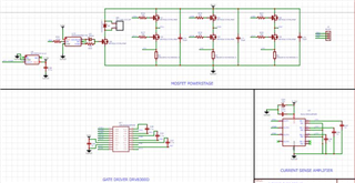
i am building a 3 phase BLDC controller for a 350Watt hub motor.

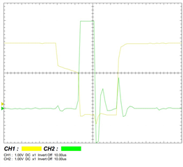
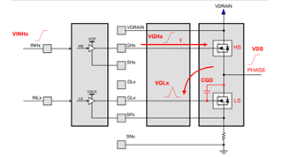
It is working fine so far but at higher target voltage (higher speeds) the mosfet are heating and there is a significant noise from switching. I am using 0.05% software deadtime but the highside mosfet seems to be not turning off immediately and is crossing the deadtime during turn off. 

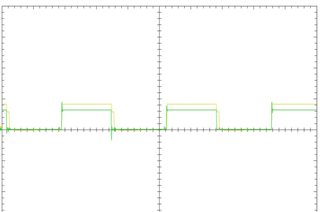
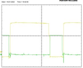
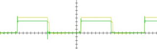
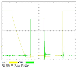
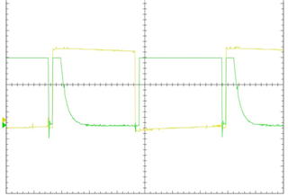
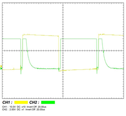
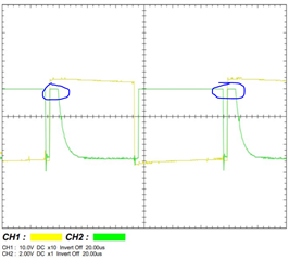
The graph below is between input signal to drv8300 ( Green waveform ) and high side output of drv8300 to mosfet ( yellow waveform ).

this issue with high side is there for all three phases. low side mosfet gate signal is perfect. 

This condition is irrespective of load.

kindly support me with this.

Thanks you,

Syed Sameeullah,

CTO @ Enarxi Innovations Pvt. Ltd.

  • Hi Syed,

    How fast are you turning on/off the external MOSFETs? We recommend a VDS slew rate no faster than 100ns; any faster can cause improper gate switching, inductive spiking, dV/dt coupling, or excessive ringing. Using a larger gate resistor or higher Qgd value MOSFETs will make the rise/fall times slower. 

    Can you share the schematic/layout of your application? Excessive heating can occur from conduction and/or switching losses. There should be sufficient copper area and thickness to thermally dissipate any power losses from the MOSFETs, especially for higher current applications. We recommend at least 10mil/amp/1oz copper thickness, and routing the motor current paths through multiple layers with direct connect vias for best thermal dissipation. 

    Resources:
    https://www.ti.com/lit/pdf/slvaf66
    https://www.ti.com/lit/pdf/slva959


    Thanks,
    Aaron

  • The following is the top layer of the layout. the bottom layer is fully ground plane ,  with necessary vias.

    kindly refer the images for the same.

    the mosfets are not heating up at dutycycle below 50%. if i increase the duty cycle to more than 50% it slowly warms up over time and attain a temperature where i am not able to touch with my bare hand for more than a minute. it takes overall 7 minutes or more to heatup.

    gate resistors are 15Ohms although when measured on track it shows 18Ohms.

    i lack information on slew rate. will look into this too.

  • Hi Syed,

    Upon quick review, I see a lot of thermal connects rather than direct connects. We do not recommend thermal connects because heat dissipation requires as much copper area as possible. Motor connections and MOSFET connections have thermal vias, so power losses will dissipate as thermal heat and is harder to dissipate when there are breaks in the copper area.

    I also do not see multiple layers for the switch nodes (SHA/SHB/SHC), so almost all thermal heat will dissipate on this copper pour. Compare to the DRV8300DIPW-EVM layout, there is multiple layers of copper for the motor current paths with 50-100 vias directly connecting the nets across layers. 


    In regards to gate drive current, 15 ohm may be a little small since max gate drive current is 750mA. I would check the VDS slew rate of the MOSFETs to determine if the FETs are being turned on too fast. Slew rates faster than 100-ns can result in inductive spiking, overshoot, bad EMI performance, or improper gate switching. 

    Furthermore, gate drive traces look pretty thin, having 15-20 mil wide traces can help with FET turn ons/turn offs by lowering parasitic inductance in the gate drive paths when switching higher gate drive currents.


    Thanks,
    Aaron


  • Hi Aaron,

    The thermal vias are between Ground of mosfet and Bottom Ground plane. there are no vias provided for SHx pads(switch nodes).

    I bellieve i have to study further into slew rate of mosfet as you had suggested. i will be testing the same and updating my results. 

    I see many designers use external Diodes across each mosfet . I wonder if adding that would help with my current issue.

    I will keep in mind the suggestions provided to upgrade my next design.

    Thanks,

    Syed

  • Hi Aaron,

    I have made few tweaks to my hardware based on the EVM design of DRV8300 as suggested by you. It seems to have improved the system performance by eliminating noise and spikes on the gate signals. Although the glitch at turn off of the high side mosfet remains.

    I have also observed that the Glitch at high side turn off of the mosfet gate is eliminated at lower switching frequencies.

    the above plot is at 20KHz switching frequency at 95% dutycycle

    the above plot is at 2KHz switching frequency at 95% dutycycle

    I suspect the Bootsrap capacitor Value as the one i am using is 100V 1uF ceramic capacitor, But in the EVM bootstrap capacitor of 25V 1uF is used.

    Could it be possible using a 100V bootstrap capacitor might be affecting the signal?

    I havent been able to check VDS signal as i do not have a IsoVu probe, Could you suggest an alternative method to check the same signal on the scope .

  • Hi Syed,

    Glad to see performance is improving. DRV8300 is rated for lower abs min specs at GHx/GLx for transients with respect to their sources. 


    100V rated bootstrap does not affect performance. 

    I'm not sure what IsoVu probe is. Can you measure SHx only with a single-ended probe? You can calculate VDS on the HS FET by calculating PVDD-SHx and VDS on the LS FET from SHx to GND. 

    Thanks,
    Aaron


  • Hi Aaron,

    i have checked between lowside gate and SHx and it looks odd.

    not sure what is causing this.

    "You can calculate VDS on the HS FET by calculating PVDD-SHx"

    i believe we need a 4 ch scope for this. I have only 2channel and cannot subtract PVDD from SHx.

  • Syed,

    Which channel is which above, and what duty cycle are you running at? What is the vertical and time divisions?

    For future since you only have 2-channel scope, can you capture these measurements zoomed in with vertical and horizonal divisions?
    1) GHx and SHx
    2) GHx and GLx
    3) PVDD and SHx

    These will help determine gate driver operation more clearly. 

    Thanks,
    Aaron

  • Green is the low side gate signal and Yellow is SHx(VDS of lowside). 

    Time Division : 20uS

    I can plot the above three parameters , will share Asap.

  • Hi Syed,

    I'll get you a more formalized response tomorrow. 

    Thanks,
    Aaron

  • Hi Syed,

    I am confused about the low-side gate signal behavior. Why is GLx going back high again in the blue circles? Is the GVDD voltage less than 10V? I would expect GLx to stay off after SHx goes high. This would indicate a shoot-through condition across the HS and LS FETs and potential damage. 

    There may be dV/dt coupling occurring when SHx goes high. This causes a rise in GLx voltage due to parasitic CGD coupling at the LS FET. Using a smaller gate drive current (increasing gate resistor value), adding dead time between GHx going low and GLx going high, and having a robust power stage layout to mitigate parasitics are ways to circumvent this issue. 

    Please share your other waveforms when you get the chance. 

    Thanks,
    Aaron