Other Parts Discussed in Thread: INA240, INA286
Hi,
I'm using a DRV8300DI (Inverted) gate driver IC and at the moment I have some trouble with the current measurement (Low-Side Measurement).
I already have an article here and I changed from the INA286 to the INA240, but still have trouble: https://e2e.ti.com/support/amplifiers-group/amplifiers/f/amplifiers-forum/1103739/noise-in-current-measurement
So I'm thinking, that it has nothing to do with the CSA, but something to do with how I switch the MOSFETs.
Problem:
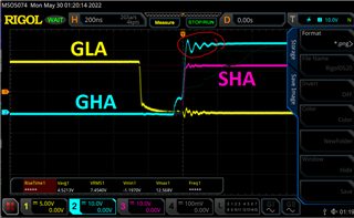
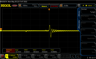
I see strong pulses on the CSA output from the INA240, where the pulses got stronger when I increased the gate resistor from 10Ohm to 39Ohm:
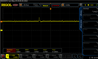
What I noticed when I increased the resistor to 39Ohm is, that the MOSFETs get warm (35°C) without any load and I have 3000mm2 for cooling.
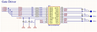
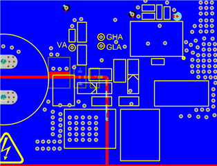
Schematics:

Layout:
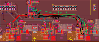
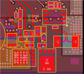
TOP
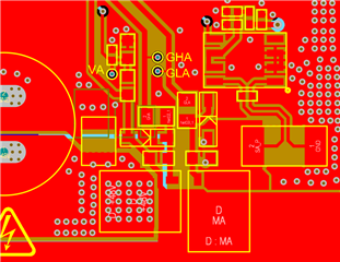
GND
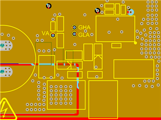
PWR
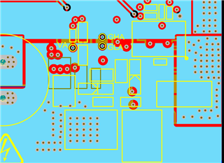
BOT
Output with 10Ohm gate resistor and 200Ohm output resistor (SHA) to GND:


Output with 39Ohm gate resistor and 200Ohm output resistor to GND:

Edit:
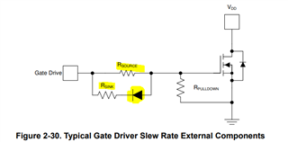
I made some more measurements today and I don't really think I have a shot through, but probably the Cds capacitance is coupling into the shunt, where the shunt has a non negligibale inductance and that leads to a glitch. The following measurement is with a spring probe over the low side shunt of 300uOhm, so that is probably the noise, that the CSA is reacting to. It is a really fast input, so I will try to use an input filter in the next design anyway. The noise comes probably from the inductance of the shunt and when the low-side switches, Coss is shorted to GND and this probably is the reaction from it.
Is it really possible, that the INA240 (and also the INA286) react with such a step response to a such fast transient?
Edit 2:
When I add an input filter to the amplifier, I can drastically reduce the glitches, so I think this really fast transients activate a step response, that is way way slower. With a better filter I think I can handle them, but my question ist now, how fast pulses on the input still lead to such a step response? Does any dirac puls give me the step response stated in the datasheet? So probably for low side shunts it would be beneficial to use a very fast differential amplifier with >10MHz bandwidth and an input filter. Since the low side fet will always shunt the Cds, there will always be a spike over the shunt and especially for low shunts and high CSA amplification, there will be less damping and this leads then to more noise on the output. I will probably go for in-phase current measurement with the INA240, but I'm unsure if this might also give problems with the 100V/V amplifier and 300uOhm shunt or do you think, the INA240 can handle this better?