This thread has been locked.

If you have a related question, please click the "Ask a related question" button in the top right corner. The newly created question will be automatically linked to this question.

INA240: High Freq dv/dt transients

Guru 54118 points
Part Number: INA240
Other Parts Discussed in Thread: TINA-TI, , TIDA-00909, INA219, INA282, INA181

Hi,

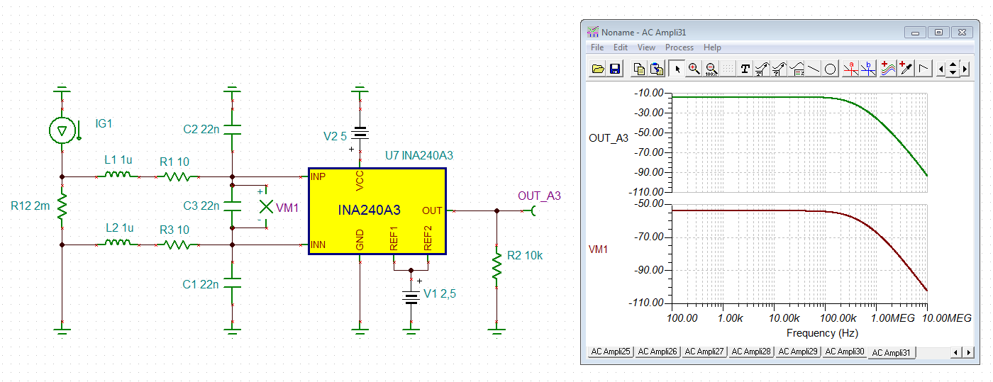
What is best way to stop high frequency 20-60mHz low side shunt EMI transients persistently passing to INA output?  Is that even possible to expect from a shunt connect into differential amplifier without TI proprietary signal isolation being present?

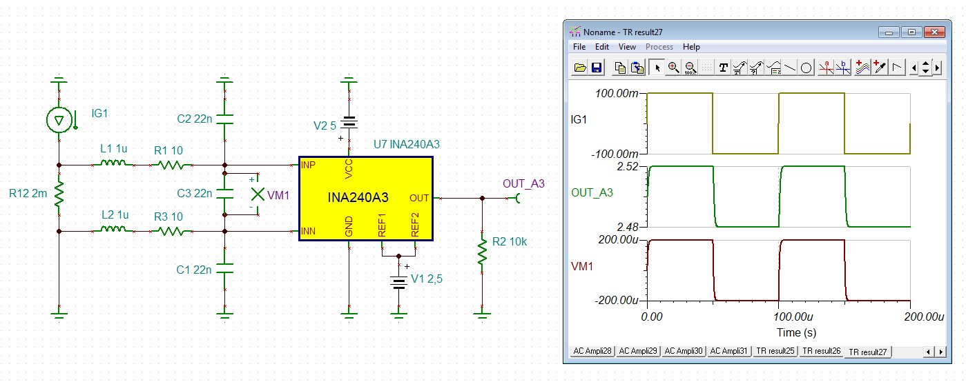
Note INA monitors same phases of DC drive signal into motor which are EMI free. So EMI (dV/dt) originates near or below ground and is not being PSRR rejected on +/-IN @-60db thus passes into output. The 3 motor drive signals are free of this EMI signal, not dI/dV/dt. Yet the INA output is plagued by high frequency amplitude pulsed EMI wave forms passing into MCU. That is effecting several MCU peripherals behavior especially SAR ADC acquisition settling time distorts conversion >400us.

INA alone simply is not stopping EMI transients no matter how or where scope probe connected to INA output on PCB, it is real trouble. 

  • Hi BP,

    the only way to get the job done is to use a rigorous passive low pass filter at the input of INA240, or by other words, BEFORE the signal enters the chip!!! The recommended filter below would work with the classical three OPAmp instrumentation amplifier. I don't know wether it also works well with the INA420 which has a somewhat different topology. The TINA-Ti simulation looks good, though, and so I would give it a try.

    Of course, you can change the time constants to your needs. But don't make the filter resistors bigger than 10R. The 1µH inductances shall be usual ferrite beads. Eventually high current ferrite beads should be used to avoid magnetic saturation due to high current flows. Depends on the signal and the interference level, of course.

    AND: It's really important to also provide common mode filtering to the input, not only differential filtering! That's why three 22nF caps can be seen:

    bp1.TSC

    bp2.TSC

    If the INA240 comes not clear with this sort of input filtering, I would use a classical three OPAmp instrumentation amplifier instead of the INA240.

    Keep in mind that the HF interference must never never never enter the chip, otherwise all is lost...

    Kai

  • Hi Kai,

    Have you read the data sheet, 240 has embedded dV/dt transient filtering. Adding input filtering precision error % rises well above shuts resistive error %. The 2mohm has 3.9% initial error, 50 A peak via Web based shunt value tester. Bit late to make input filter changes after several costly PCB were made for Johanson's X2Y EMI (10n) input filter.
     
    Previously for kicks tested 10 ohm, 10n-100n ceramic cap filter made no direct impact to stop EMI. Only moving INA several inches away from copper metal shunt made any difference to reduce peak EMI. You can check TIDA-00909 engineer added EMI filter when INA240 should block motor EMI by design. Something is wrong with 240 embedded filter design, when low side monitoring the datasheet claims of grounded REF1/2 pin behavior defies CUT analysis.

  • Kai check this out! s21plotter.johansondielectrics.com/ 160X07W103MV4T

  • Hi BP,

    the circuit I have simulated is only an example circuit using the TINA-TI reference design.

    The input filter should contain some ferrite beads. They offer an impedance of 100...1000R in the frequency range of interest. This is much more than a 10R can offer. I have the 10R resistor only added to prevent the LC-filter from ringing. It's effect on the filtering is minimal.

    Of course, moving the INA input a bit away from the noisy shunt is a good idea. To have some shielding, as well. But it cannot be a replacement for a robust input filter.

    I think that the "dV/dt transient filtering" feature mentioned in datasheet is something added by the marketing people. How shall this work without affecting the overall linearity of chip? I would not rely on that statement. I think it's the distortion plot in figure 24 of datasheet which is telling the truth.

    Again, with HF interference at the input of INA219 I wouldn't even start to experiment without a robust input low pass filter. Equally what the datasheet is telling.

    Kai
  • Hi BP101,

    This is a question related to PCB design rather than specifically to current sensing device itself. Proper PCB design is just as important in order to take advantage of a high performance IC.

    Ideally we want only the input signal to be gained up and passed to the output. If nothing else couples to the INA output, it should be fairly free of these high frequency disturbances. Switching disturbances happen at the transitions and should only last for a couple of uS. This is achieved by the dv/dt rejection offered by the INA240. The device bandwidth is limited and should filter out MHz components, only if all the MHz components enter through the input. But, if the high frequency disturbances couple to the output through other means, there is nothing the device can do.

    In reality, no circuit node can exist in a vacuum, as a result such high frequency disturbances show up through coupling. This is where it is important to follow best practices in designing switching circuits. Some examples are – separation between switching nodes and quiet nodes, minimizing recirculating current loops, reducing parasitic inductance and separation of grounding.

    It is one of the situations where even if best practices are followed, it is not guaranteed that the PCB will work; but if the guidelines are not followed, the PCB for sure will not work.

    If I remember correctly, we looked at some images of your PCB. Feedback was provide, did any of that help? Did you have a chance to adopt and hopefully improve your circuit board?

    Regards, Guang

  • Hello Guang Zhou,

    Guang Zhou said:
    Switching disturbances happen at the transitions and should only last for a couple of uS. This is achieved by the dv/dt rejection offered by the INA240

    The 240 is not rejecting (peak) shunt dV/dt 20mHz-125Mhz range simply being amplified on output. The ringing dV/dt is the amplified high voltage EMI (cyclic/random) and way above the relative normalized 20v/v gain.

    Is EMI considered a transient being the amplitude of only a few cycles shoot way above the normalized output signal threshold?

    How can shunt current suddenly jump several hundred mV on 240 output during EMI events if PSRR is actually functional -20db to -60db down. Seemingly laboratory choosing AC sine wave +/-IN is a poor way to prove dV/dt is being rejected at higher PSRR frequencies 20-125Mhz transient pulse reaction periods. Obviously a BLDC motor produces frequency range the PSRR of 240 is not blocking, rather amplifying instead. The 240 ain't blocking EMI 20-125mHz range it only amplifies the events 20v/v. 

    Guang Zhou said:
    it is not guaranteed that the PCB will work; but if the guidelines are not followed, the PCB for sure will not work

    The datasheet guide lines for PCB layout fail to mention anything about copper foil being present under the IC or how it may help or otherwise deviate IC from datasheet facts. Seemingly datasheet is a bit sloppy in scope omits warnings TSSOP package perhaps should not exist next to high reverse current traces or sources? How would anyone know the TSSOP might be susceptible to magnetic lines of force of the shunt in the typical Kelvin connection? Rules for making Kelvin connections warn to keep input traces short as possible, proximity of TSSOP closes in on shunt mounting locations, Kelvin rules first apply. Again not one warning in older datasheets shunt proximity TSSOP package issues are know to exist, has that part of datasheet been updated yet? Has TI bothered to further test the 240 and improve the datasheet?

    Guang Zhou said:
    If I remember correctly, we looked at some images of your PCB. Feedback was provide, did any of that help? Did you have a chance to adopt and hopefully improve your circuit board?

    Again there is nothing wrong with circuit board layout according to INA datasheet. Yet shunt bound cyclic motor EMI is simply being amplified by INA. No matter how INA exist on any PCB surface even isolated vertical PCB attached to shunt, very same cyclic motor EMI randomly peaks way above normalized output gain. The odd thing is INA282 was producing similar much lower EMI peak events, REF tied to ground output signal remained above 0v. The 240 output REF tied to ground output peaks below 0v, during cyclic random EMI events >-2v typical. Again EMI events are not persistent and deviate way above normalized output signal effecting ADC acquisitions. The only thing to reduce cyclic EMI was an extensive 22n decoupling cap to ground. That also made transients hang longer tripping comparator faults in the process. At present there in no added capacitance load INA output other than TDK ferrite (0.3 DCR) reduce peak EMI pulses @100mHz, 2" long trace over to MCU 4R87k into 330nH choke near ADC input. 

    Below 20 pole magnet motor may produce similar EMI as our large 36 pole BLDC. Perhaps TI engineers can test 240 is doing what it claims in datasheet. It's not enough to laboratory test an IC as PSRR of dV/dt frequency range inside EMI events must hold true under real world conditions, not with only inductive motors but larger PM machines too.

    https://www.ebay.com/itm/EV-motor-DirectDrive-BLDC-20kw-peak40Kw-100V-or-160V/223069829296?ssPageName=STRK%3AMEBIDX%3AIT&_trksid=p2060353.m1438.l2649

  • Hello Kai,

    Perhaps looking at different datasheet, there is no figure 24. Are you aware Tina may produce incorrect transient analysis if more than one INA is present in schematic view. The original 240 transient analysis had 4 devices, often produced incorrect results. Agree must be marketing fluff but the low end current error is nearly 3.9% without input filter.

    wondering can you please test A1 PSRR (20-125mHz) range with 330nH ferrites L1/L2, REF1/2 GND, signal 12.5kHz PWM, low side monitor? I have a few 330nH (0402) on hand and several XY2 10nf cap C3 position can perhaps reduce clutter of several 22n.

    Past tested 22n-100n across +/-IN which only made shunt/motor transients trip any one of 3 fault comparators much sooner.  That is sort of the other issue where the comparators fault threshold is close to the random cyclic EMI peaks. BTW 3v2 output rail is the ADC full scale 2mohm, A1 20v/v, 80 amps peak, 40mV/A. Output level actually ends up a bit higher than 40mV/A adding TDK MMZ1608B102CTA00 (0.6ohm) ferrite reduce peak EMI @100Mhz.  The TDK output ferrite only reduces the EMI envelop frequency it seems.

  • Hi BP101,

    The data sheet is a governing document for the IC only, it is not meant to dictate system design including layout. It can suggest application and design techniques, but in no way can it cover all aspects of every possible application.

    That said, I’m trying really hard to see how to help you move forward. I think it might be helpful for you to check out a few other products, the possible outcome might be (1) you are convinced that this is not a unique problem due to INA240, or (2) some device works better for you. I don’t know the answer at this point. The reason is that in a low side current sensing configuration, the dv/dt feature really is not required. As long as the IC is fast enough with a REF pin (which you might not need as you mentioned), it is probably OK. The other requirement is that the common mode range includes below ground for at least a few 100mV. You seem to be fairly familiar with our portfolio, please go to TI.com to check out the wide selection of current sense amplifiers. You may start with INA181 for example.

    Regards, Guang

  • Hi BP,

    I mean this figure here:

    I have deleted the other three INA240s before doing the simulations. Does this fix the issue?

    bp3.TSC

    bp4.TSC

    Kai

  • Hi Kai,

    Thanks to re-run simulation :-)

    Oh that Figure 24 stuck way out in the PDF away from all the other graphs. Seemingly fails to apply @12.5kHz current measures, high frequency EMI passing 240 output should roll off by design. Notice THD curves upward above the frequency range of where our current measure occur. It would seem THD should be very low @12.5kHZ and for most part it is very clean during actual current events. Yet THD grows outside those event as dV/dt EMI drives THD >100% counter to Fig. 24 and claim of high immunity. It would seem >10% THD should be outside 400kHZ band width and not produce high frequency EMI as it does, fails to (reduce) output level as text states. Fact is the exact opposite to Fig.24 paragraph occurs. THD actually gains up noise >400kHz in output open loop passing high level EMI into ADC input saturation regions.

    EMI roll off need be 20mHz to >125mHz range, Johanson S21 plotter (10n) barely touches -50db @100mHz. Certainly one would think X2Y alone should reduce shunt EMI without 10R or 330n inductors ferritesare not multi layer inductors, high current ferrites produce impedance roll off of high frequency so Tina was not producing same results as ferrite bead with inductor might. Seemingly we need to use the spectrum analyzer tool in Tina to know how THD is effected graphically to noise, SNR. If I recall correctly @12.5kHz(80us) periods (PWM) the SNR level (THD) seems to hiccup near -60db.

    The bottom ADC full scale range simulation 2mohm shunt appears very correct. 

  • Hi Kai,

    I meant to say high current ferrite bead above post but Tina Spice models don't include ferrites. TDK/Murata last check did not support a Spice macro to import. Odd observation Johanson S21 plotter indicates 10n signal starting 0Hz rolls back up around 110Mhz -52db and Tina has VM1 starting -52db 1kHz. The difference of VM1 just from adding L1/L2 and R1/R3 (10R) seems somewhat questionable, does it not?

    Did you have chance to try spectrum/signal analyzer (T&M) Tina toolbar? Did you find it useful to determine changes in power density spectrum after adding +/-IN components?  Hint click the data arrow -> to export the spectrum analyzer graph plots of VM1, others. I used the function generator as source 12.5kHZ output to IG1, channel OUT_A1. Spectrum analyzer produces some very interesting plots of model signals.

  • Hi BP,

    unfortunately, the power analyzer tool of TINA-TI doesn't work for me. The processor only heats without doing anything useful...

    The impedance of a ferrite bead can simulated pretty well with such a model:

    Repeating the simulations with this "real" ferrite bead shows the following results:

    Of course, the next step would be to model the "real" 10n input caps with their inductances and so on. No simulation is absolutely correct. But I think, and that was the deeper sense of these simulations, you can see that using ferrite beads can be extremely helpful, even if the ferrite bead isn't a perfect component either.

    Kai

  • Hi Kai,

    I have quad core Intel 2.8Ghz overclocked and even the tool locks up Tina at times if select other than single trigger source. Part of my hesitation was Tina Spice library does not have ferrite beads. Seemingly an inductor can not exactly simulate the effects of EMI reducing ferrite beads. Seemingly Tina simulation has to be DC not AC or the INA240 does not produce the same plot results that occur via real time PWM driving DC transients.

    The 330n inductors are multilayer stacks with outer ferrite powder core, ferrite beads are not inductive according to the datasheets they are resistive devices. If the intent was to place ferrite beads in series to reduce EMI, the +/-IN impedance becomes more the issue in the presence of EMI @20mHz -100Mhz range. The smaller beads (0402) range 15-30Zohms @100mHz, <0.4ohms DCR.
  • Hi BP101,

    We have an E2E forum devoted to simulation and tools. I think you’ll receive expert support there regarding simulation questions.

    As I said in previous posts, I think the issue is beyond INA240 itself.

    Regards, Guang

  • Hi Guang,

    Good part of transient EMI was coming from the AGND loop into ADC separated from MCU digital (DGND) via <20mohm or <4mOhm ferrite beads. The 240 output pulse peaks <5v dropped to <500mV open loop gain after ferrite bead replaced with 0R, <50mohm DCR. Tested yesterday 10nf X2Y cap direct on 240 input did not seem to do any good that could be noticed on scope probe. The negative pulses below ground <200mv peak after bead removal are seemingly harmless.

    Why the 240 open loop output gain became unconstrained from AGND plane 240 connected to remains a mystery. Also contrary to how a ferrite bead is supposed to reduce high frequency EMI, it actually produced high EMI from 240 output. That described AGND method was past disclosed to forum, not a word from experts. Hind sight being impedance between ADC internal LDO supply was somehow increasing via DGND even though ADC (AGND) was on the same ground plane 240 used. That was the ADC to blame in my opinion, not the 240.